Interface Addressing Explained: Memory-Mapped vs Isolated I/O with Worked Examples
Understand what an interface address selects, how memory-mapped and isolated I/O differ, and why partial decoding creates multiple addresses for the same register.
KnowledgeGate Team
Exam prep & CS education
Updated 23 Sep 20266 min read
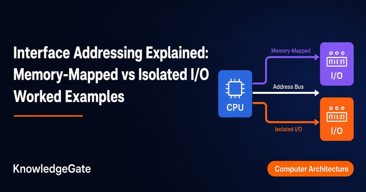
Connecting a peripheral to the bus does not make it addressable. In I/O interface addressing, the CPU selects registers exposed by the interface, placed either in the memory address space or in a separate I/O space. Register ranges and the aliases created by partial decoding follow from the address allocation.
What an I/O interface address actually selects
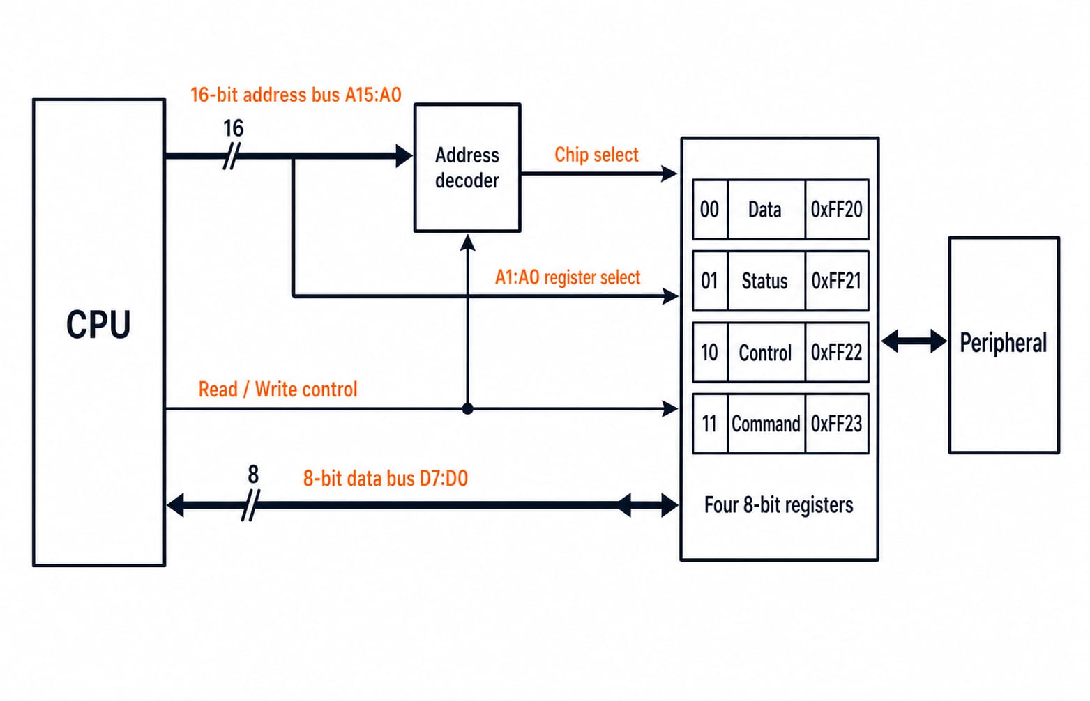
The path is CPU <-> system bus <-> address decoder <-> I/O interface <-> peripheral. An interface exposes data, status, control and command registers. The CPU addresses these registers, not the peripheral as one indivisible object.
What those registers contain, bit by bit, and what a complete transaction through them looks like is traced in Computer Interfaces in COA; this post asks only how the decoder reaches them.
Four 8-bit registers in a byte-addressable machine normally require four addresses. Do not confuse this with the CPU operand choices in Addressing Modes and Instruction Formats. An operand addressing mode finds an operand, while interface addressing decides which I/O register responds.
Every transfer has three distinct parts. The address selects the interface and one of its registers, the read or write control signal gives the direction, and the data bus carries the value. Address lines do not carry the data.
How the two schemes differ at the decoder
Both schemes address interface registers, but they place those addresses in different spaces.
Point | Memory-mapped I/O | Isolated I/O |
|---|---|---|
Address space | Interface registers share the memory address space | Interface registers use a separate port space |
Instructions | Normal memory operations access the registers | Architecture-specific I/O operations access the ports |
Control signals | The transfer is a memory read or write | The processor distinguishes an I/O read or write |
Effect on memory addresses | Assigned interface addresses occupy part of the memory map | Port addresses do not consume memory addresses |
Which scheme a designer should choose is settled in Input Output Organisation in COA; what a mapped block does to the address COUNT is exactly this post's decoder arithmetic, worked below. Here the only question is which register responds to which address.
For either scheme, count addressable registers, respect byte or word addressability, and never mix a memory address count with an isolated port count.
Worked example 1: Allocate two interfaces in both schemes
Consider a byte-addressable system with a 16-bit memory address bus and an 8-bit data bus. Interface A has four 8-bit registers, and B has eight. In memory-mapped I/O, A starts at 0xF000 and B at 0xF008. In an 8-bit isolated port space, they start at 0x20 and 0x30.
These address values define this example, not universal hardware.
For a block of N consecutive registers:
end = base + N - 1
The memory-mapped ranges are therefore:
A ends at
0xF000 + 4 - 1 = 0xF003, so A occupies0xF000-0xF003.B ends at
0xF008 + 8 - 1 = 0xF00F, so B occupies0xF008-0xF00F.The addresses
0xF004-0xF007form a four-address gap. They belong to neither interface under the stated allocation.
A 16-bit byte address has 2^16 = 65,536 possible values, from 0x0000 to 0xFFFF. A and B contain 4 + 8 = 12 assigned register addresses. If RAM responds at every other address, the remaining memory capacity is 65,536 - 12 = 65,524 byte addresses.
Hardware may instead reserve the complete 0xF000-0xF00F decoder window. It contains 0x10 = 16 addresses, including the gap, so 65,536 - 16 = 65,520 remain for RAM. The hardware assumption changes the answer.
An 8-bit isolated port number provides 2^8 = 256 ports, from 0x00 through 0xFF. A occupies 0x20-0x23, and B occupies 0x30-0x37. All 65,536 memory addresses remain because the registers use a separate port space. Memory-mapped I/O consumes 12 assigned addresses, or a 16-address window under the second assumption, while isolated I/O consumes none of the memory map.
Worked example 2: Full decoding, partial decoding and aliases
Now take the four-register memory-mapped interface at 0xD820-0xD823. With full decoding, chip-select is asserted only when the upper address lines have the required value:
These address values define this example, not universal hardware.
A15:A2 = 11011000001000
The endpoint check is exact:
0xD820 = 1101 1000 0010 00000xD823 = 1101 1000 0010 0011
The upper 14 bits remain the same, while A1:A0 changes from 00 to 11 to select Data, Status, Control or Command.
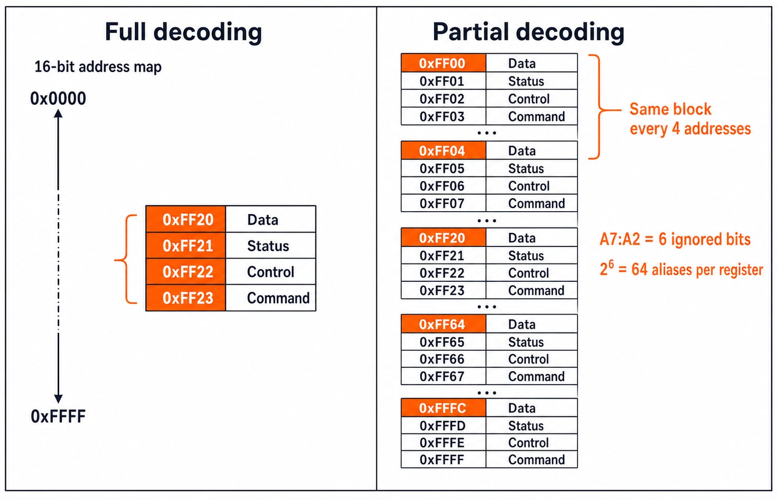
Now suppose the decoder checks only A15:A8 = 11011000, passes A1:A0 to the register selector, and ignores A7:A2. There are six ignored bits, so each physical register responds to:
aliases = 2^6 = 64 address values
The four-register block consequently appears 64 times across 0xD800-0xD8FF. The Data register, selected when A1:A0 = 00, responds at 0xD800 + 4k for k = 0, 1, ..., 63. Examples include 0xD800, 0xD804, 0xD820, 0xD864 and 0xD8FC.
Partial decoding needs less logic but creates mirrored addresses. The aliases cannot safely select something else because the interface will also respond. They are multiple addresses for the same physical registers, not extra registers.
How exams turn interface addressing into a calculation
Use this routine for exam-style forms of the problem:
Identify whether the address belongs to memory-mapped or isolated I/O.
Note the address-bus width and whether the system is byte-addressable or word-addressable.
Count addressable registers, not connected devices.
Compute the inclusive range with
end = base + N - 1.Count ignored decoder bits and calculate
aliases = 2^k.Check which instruction or control signal distinguishes a memory cycle from an I/O cycle.
Three quick checks apply the rules. A 10-bit isolated-I/O address provides 2^10 = 1,024 ports. Sixteen byte registers from 0xD200 end at 0xD200 + 16 - 1 = 0xD20F. Ignoring three address bits produces 2^3 = 8 aliases per register.
GATE learners can place these calculations inside their wider preparation through the GATE category page. Treat them as exam-style forms for practice, not as a claim about marks, frequency or a guaranteed paper pattern.
Traps that change an otherwise correct answer
The first trap is forgetting that a range is inclusive. Four registers beginning at 0xD820 end at 0xD820 + 4 - 1 = 0xD823, not 0xD824.
Other common errors are easy to detect once you name them:
Counting one peripheral instead of its four or eight addressable registers.
Subtracting isolated port addresses from memory capacity even though the spaces are separate.
Treating a word-addressable machine as byte-addressable without adjusting what one address selects.
Assuming an address is free just because it lies outside the intended range.
That last mistake matters under partial decoding. In the worked example, 0xD864 has A1:A0 = 00 and therefore selects the Data register, even though it lies outside the intended 0xD820-0xD823 block. As a final sanity check, confirm that the inclusive range size equals the register count and that k ignored bits produce exactly 2^k address images per register.
The short version and the next useful step
The CPU addresses registers in an I/O interface, not an undivided peripheral. Memory-mapped I/O places those registers in the memory map, while isolated I/O gives them a separate port map. Ignored decoder bits create aliases for the same physical register. Keep the two formulas end = base + N - 1 and aliases = 2^(ignored bits) ready.
For a structured GATE preparation route, use GATE Guidance by Sanchit Sir. For a broader Computer Science concept path, ZERO TO HERO is the relevant next option. To see decoded addresses put to work in a running transfer, continue with Direct Memory Access (DMA) Explained, where a controller generates its own successive addresses instead of receiving them from an instruction.
Finally, redraw the 0xD820-0xD823 decoder and recompute the result when four address bits, rather than six, are ignored. Your self-check is 2^4 = 16 aliases per register.
Keep learning

Multiprocessor Classification: Flynn Taxonomy, Memory Models and Exam-Style Worked Examples
Learn how to choose the right multiprocessor classification axis, then solve a four-lane SIMD trace and a NUMA average-access-time problem step by step.
Updated 27 Sep 20266 min readComputer Organization & Architecture

Interrupt-Driven I/O Explained: CPU Handshake, Worked Timing Example and GATE Traps
Trace an interrupt from device request to return-from-interrupt, then compare polling, per-event interrupts, and DMA through worked timing examples.
Updated 25 Sep 20267 min readComputer Organization & Architecture

Instruction Structure in Computer Organization: Fields, Encoding and Exam Problems
Learn how opcode, register, mode and displacement fields divide an instruction word. Follow checked examples for address forms, decoding and expanding opcodes.
Updated 22 Sep 20265 min readComputer Organization & Architecture

Disk Structure and Disk Addressing for GATE: CHS, LBA and Worked Examples
Use one consistent disk geometry to connect platters, surfaces, tracks and sectors with capacity, CHS-to-LBA conversion, address width and access time.
Updated 21 Sep 20265 min readComputer Organization & Architecture