Logic Circuit Analysis MCQs: 12 Solved Questions on Gates and Boolean Functions
Practise 12 logic circuit analysis questions with fresh explanations covering minterm sets, bubbles, hazards, XOR patterns, and equivalent Boolean forms.
KnowledgeGate Team
Exam prep & CS education
Updated 13 Sep 20267 min read
Gate symbols are usually familiar. The trouble is that one missed bubble, a wrong AND or OR set operation, or unnoticed XOR cancellation changes the complete answer. Minterm-set arithmetic, NAND networks, hazards, XOR and XNOR, and equivalent SOP and POS forms all depend on correct signal tracing. Write every intermediate signal before reading each answer. Use Digital Electronics MCQs for wider practice, or browse GATE CS Exam Preparation for the course route.
Related reading: logic circuit analysis and Boolean minimisation.
1. Logic circuit analysis: the three-line method before solving
First, label every gate output. Second, translate each NOT, NAND or NOR bubble immediately, with the complement covering the full gate expression. Third, choose the cheapest representation for the question. For fixed truth values, propagate 0 and 1. For minterm functions, AND means intersection, OR means union, NOT means complement within the stated variable universe, and XOR means symmetric difference. Before comparing options, fix the variable order because decimal minterm indices depend on it. Keep parentheses until every De Morgan complement is distributed, and test a doubtful expression on one input row.
For example, if P=Σ(1,2,5) and Q=Σ(2,4,5), then P·Q=Σ(2,5), P+Q=Σ(1,2,4,5), and P⊕Q=Σ(1,4). XOR removes minterms present in both inputs. If these translations are not yet automatic, review the Boolean Algebra and K-map Minimization Guide.
2. Minterm-set circuit MCQs: Questions 1-3
Question 1: combine AND, OR and XOR on four minterm sets
Asked in GATE 2024, Set 2. Solved question.
Consider 4-variable functions f1, f2, f3, f4 expressed in sum-of-minterms form as given below.
f1 = ∑(0,2,3,5,7,8,11,13)
f2 = ∑(1,3,5,7,11,13, 15)
f3 = ∑(0,1,4,11) f4 = ∑(0,2,6,13)
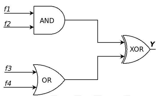
With respect to the circuit given above, which of the following options is/are CORRECT?
A.
𝒀 = ∑(0,1,2,11,13)B.
𝒀 = Π(3,4, 5,6,7,8,9,10,12,14,15)C.
𝒀 = ∑(0,1,2,3,4,5,6,7)D.
𝒀 = Π(8,9,10,11,12,13,14,15)
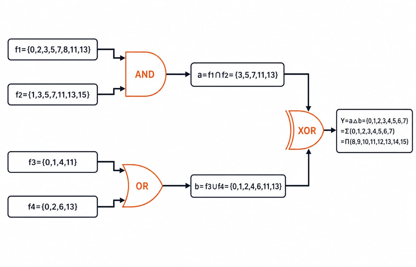
Answer: C and D. The AND gives a=f1∩f2={3,5,7,11,13}. The OR gives b=f3∪f4={0,1,2,4,6,11,13}. Their symmetric difference is {0,1,2,3,4,5,6,7}, matching C. Its zero indices are 8 through 15, so D is the equivalent maxterm form.
Question 2: translate a three-input circuit into minterms
Asked in GATE 2020. Solved question.
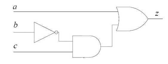
Consider the Boolean function . Which one of the following minterm lists represents the circuit given above ?
A.
\(z=\sum (0,1,3,7)\)B.
\(z=\sum (1,4,5,6,7)\)C.
\(z=\sum (2,4,5,6,7)\)D.
\(z=\sum (2,3,5)\)
Answer: B. The circuit is z=a+b'c. In variable order a,b,c, a=1 produces minterms 4,5,6,7. With a=0, b'c=1 only for 001, minterm 1. Thus z=Σ(1,4,5,6,7).
Question 3: use intersection before XOR cancellation
Asked in GATE 2019. Solved question.
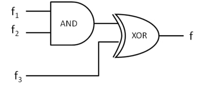
Consider three 4-variable functions f1, f2, and f3, which are expressed in sum-of-minterms as For the following circuit with one AND gate and one XOR gate, the output function can be expressed as:
A.
\(\Sigma(7,8,11)\)B.
\(\Sigma(2,7,8,11,14)\)C.
\(\Sigma(2, 14)\)D.
\(\Sigma (0,2,3,5,6,7,8,11,14,15)\)
Answer: A. The AND stage is {2,8,14}. XOR with {2,7,11,14} cancels common minterms 2 and 14, leaving {7,8,11}. Treating XOR as OR wrongly retains both and points towards B.
3. NAND reduction and hazard MCQs: Questions 4-6
Question 4: identify every equivalent output expression
Asked in GATE 2025, Set 2. Solved question.
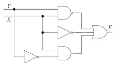
Consider the following logic circuit diagram. Which is/are the CORRECT option(s) for the output function 𝐹?
A.
\(\overline{X Y}\)B.
\(\overline{X}+\overline{Y}+X \overline{Y}\)C.
\(\overline{XY}+\overline{X}+X \overline{Y}\)D.
\(X+\overline{Y}\)
Answer: A, B and C. The final OR inputs are p=(XY)', q=X', and r=XY'. Therefore F=(XY)'+X'+XY'=(XY)', since (XY)'=X'+Y' already contains X'. B absorbs XY' into Y', while C absorbs both extras. D fails for X=1,Y=1.
Question 5: test whether any input is redundant
Asked in GATE 2005. Solved question.
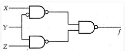
Consider the following circuit. Which one of the following is TRUE?
A.
f is independent of XB.
f is independent of YC.
f is independent of ZD.
None of X, Y, Z is redundant
Answer: D. The final NAND gives f=((XY)'(YZ)')'=XY+YZ=Y(X+Z). At Y=1,Z=0, f=X; at Y=1,X=0, f=Z; at X=1,Z=0, f=Y. Each input can change the output, so none is redundant.
Question 6: choose a static-1-hazard-free cube cover
Asked in GATE 2006. Solved question.
Consider a Boolean function f(w, x, y, z). Suppose exactly one input is allowed to change at a time. If f is true for two input vectors i1 = (w1, x1, y1, z1) and i2 = (w2, x2, y2, z2), and i1 and i2 differ in exactly one bit position, we want f to remain true during the transition without becoming false momentarily. Let f(w, x, y, z) = ∑(5, 7, 11, 12, 13, 15). Which of the following cube covers of f ensures this required property?
A.
w'xz, wxy', xy'z, xyz,wyzB.
wxy,w'xz,wyzC.
wx(yz)', xz, wx'yzD.
wxy', wyz, wxz, w'xz, xy'z, xyz
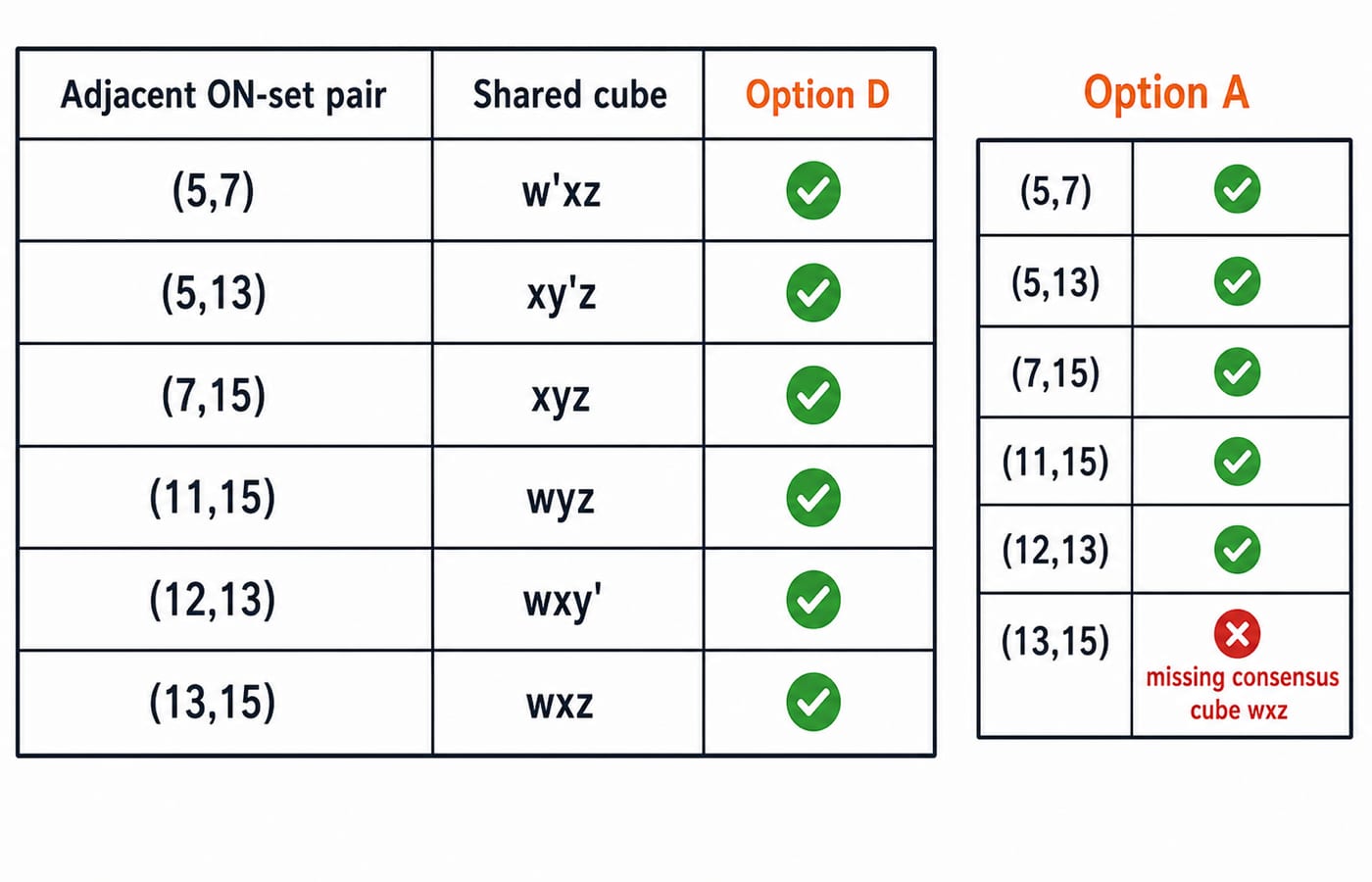
Answer: D. The adjacent ON-set pairs (5,7), (5,13), (7,15), (11,15), (12,13), (13,15) are covered respectively by w'xz, xy'z, xyz, wyz, wxy', wxz. A misses the last pair, so wxz is decisive.
4. Reverse-engineer a missing function and convert a circuit to POS: Questions 7-8
Question 7: infer f3 from the required output set
Asked in GATE 1997. Solved question.
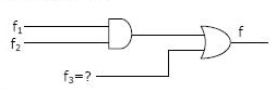
Consider a logic circuit shown in figure below. The functions f1 ,f2 and f (in canonical sum of products form in decimal notation) are : f1(w,x,y,z) = ∑ 8,9,10 f2(w,x,y,z) = ∑ 7,8,12,13,14,15 f(w,x,y,z) = ∑ 8,9 The Function f3 is
A.
∑9,10B.
∑9C.
∑1,8,9D.
∑8,10,15
Answer: B. The circuit gives f=(f1·f2)+f3. The intersection is {8}, while the required output is {8,9}. Therefore f3 must add 9 without adding another index, so f3=Σ(9).
Question 8: convert a mixed gate network into POS
Asked in ISRO 2020. Solved question.
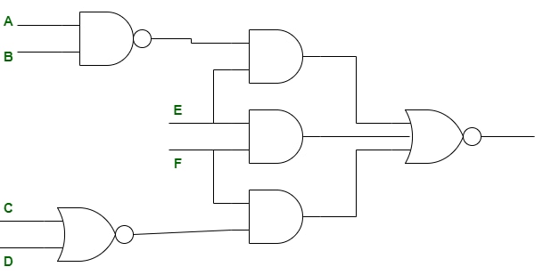
Consider the following circuit The function by the network above is,
A.
(AB)'E + EF + (CD)'FB.
(E' + ABF')(C + D + F')C.
((AB)' + E)(E' + F')(C + D + F')D.
(A + B)E' + (EF)' + CDF'
Answer: B. The final NOR complements S=(AB)'E+EF+(C+D)'F. De Morgan gives S'=(AB+E')(E'+F')(C+D+F'). Applying (X+Y)(X+Z)=X+YZ to the first two factors yields (E'+ABF')(C+D+F'). A is only the signal entering the final NOR.
5. Recognise XOR and simplify NAND/NOR circuits: Questions 9-10
Question 9: recognise the two-product XOR pattern
Asked in UGC NET 2013, December. Solved question.
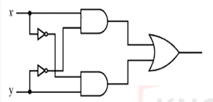
What will be the output if following logic diagram?
A.
x OR yB.
x AND yC.
x XOR yD.
x XNOR y
Answer: C. The two AND outputs are xy' and x'y. Their OR is xy'+x'y, the canonical XOR expression. At x=1,y=1, both products are 0, ruling out OR and XNOR.
Question 10: reduce a NAND-NOR-NOR circuit
Asked in UGC NET 2018. Solved question.
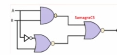
Find the Boolean expression for the logic circuit shown below: (1-NAND gate, 2-NOR gate, 3-NOR gate)
A.
ABB.
AB'C.
A'BD.
A'B'
Answer: A. Gate 1 gives (AB)'=A'+B', and gate 2 gives (A+B')'=A'B. The final NOR is ((A'+B')+A'B)'. Absorption reduces its inside to A'+B', whose complement is AB. Never remove a gate-output bubble before writing its full complemented expression.
6. Constant outputs and equivalent forms: Questions 11-12
Question 11: evaluate XOR with a constant and a complement
Asked in NVS 2019. Solved question.
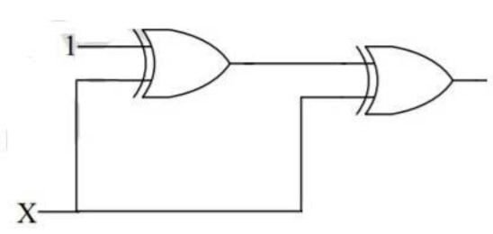
What will be the output of the following digital circuit, where X′ represents the complement of the binary variable X?
A.
0B.
1C.
X′D.
X
Answer: B. First, 1⊕X=X'; then X'⊕X=1. For X=0, the stages give 1⊕0=1, then 1⊕0=1. For X=1, they give 1⊕1=0, then 0⊕1=1.
Question 12: prove that SOP and POS describe the same output
Asked in DSSSB 2021, PGT. Solved question.
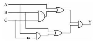
What is output of Y in the given circuit? I. BC+AC' II. (A+C)(B+C')
A.
Only IB.
Only IIC.
Both I and IID.
Neither I nor II
Answer: C. The circuit is Y=(A+BC)(B+AC'). Expansion gives AB+AC'+BC; the consensus term AB is absorbed, leaving BC+AC', statement I. Statement II expands to the same three terms and reduces identically. For A=1,B=0,C=1, the circuit, I and II each give 0.
Continue with Combinational Circuits: MUX, Decoders, Adders if you need more gate-to-expression practice.
7. Logic circuit analysis score map and next step
Misses in Questions 1 to 3 mean you should practise minterm-set operations. For Questions 4 and 5, slow down at NAND bubbles and prove dependence with counterexamples. Question 6 needs consensus coverage for every adjacent ON-set pair. Question 7 tests working backwards from the required output, while Question 8 tests conversion to POS. For Questions 9 to 12, memorise XOR forms, then still verify them algebraically.
Use the live Digital Electronics MCQs hub for another mixed set. Choose GATE Guidance by Sanchit Sir when you need the full Digital Electronics sequence before more practice. The short version: label each intermediate signal, choose truth values or minterm sets deliberately, and test any expression that only looks equivalent with one counterexample.
Keep learning
Special Logic Circuits MCQs: 12 Solved Questions on Adders, Encoders, PLA and DAC
Solve 12 special logic circuits MCQs covering recognition, hardware counts, Boolean identities and numerical calculations. Each answer includes the reasoning you should reproduce in an exam.
19 Sep 20268 min readDigital Electronics MCQs
Function Equivalence MCQs: 12 Solved Boolean Algebra Problems
Solve 12 function-equivalence questions step by step, from De Morgan's law and absorption to minterm sets, counterexamples and a four-option MSQ.
Updated 17 Sep 20268 min readDigital Electronics MCQs

CLA & Arithmetic Logic MCQs: 10 Solved Questions with Explanations
Solve ten CLA and arithmetic logic MCQs with compact workings for carry equations, timing paths, hardware sizing and operand-pair counting.
Updated 16 Sep 20267 min readDigital Electronics MCQs
Sync Counter Design MCQs: 11 Solved Questions on Modulus, State Sequences and Excitation Logic
Solve 11 synchronous-counter questions covering modulus boundaries, repeated outputs, common-clock tracing, excitation equations, enables and composite states.
Updated 14 Sep 20267 min readDigital Electronics MCQs