Logic Circuit Analysis: Boolean Simplification and Worked Examples
Learn a repeatable way to trace combinational circuits, simplify their Boolean expressions, and verify the result. Two worked examples cover a three-input network and a four-NAND XOR.
KnowledgeGate Team
Exam prep & CS education
Updated 18 Sep 20265 min read

A gate diagram can look harder than its Boolean expression when one signal branches, is complemented, and reconverges. Visual intuition is risky. Analyze each circuit node by node, simplify the three-input circuit, and decode the NAND-only circuit from internal values. Verify each result independently.
Related reading: Boolean function equivalence and XOR and XNOR gates.
1. What Logic Circuit Analysis Actually Requires
In a combinational circuit, a fixed input vector determines every node and the output. A sequential circuit differs because stored state also affects its response.
Standard Boolean notation uses the following symbols:
+means OR.Juxtaposition or
.means AND.A prime means NOT, so
B'is the complement ofB.⊕means XOR.
Fan-out means the same signal feeds several gates. It does not create independent variables.
Use three passes. First, label every gate output. Second, translate each gate into an equation. Third, evaluate or simplify, then verify independently. Start with Logic Gates in Digital Electronics when gate symbols, truth tables, or hardware details are the weak point. A connected-network problem requires a different sequence: label its internal nodes and follow them to one output.
2. Worked Example 1: Trace and Simplify a Three-Input Circuit
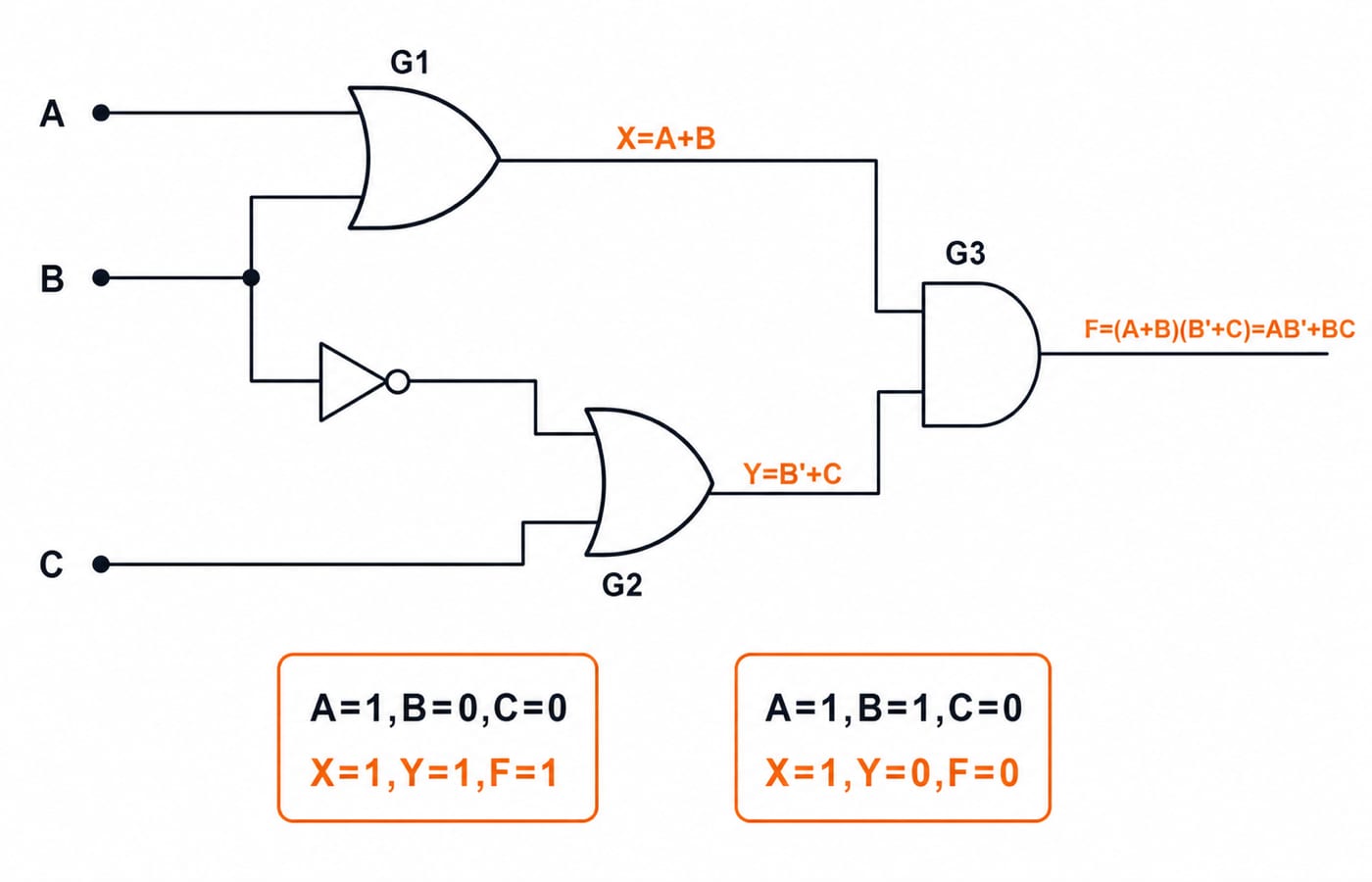
Take inputs A, B, and C. Gate 1 is an OR gate:
X = A + B
Gate 2 complements B and ORs it with C:
Y = B' + C
Gate 3 ANDs the two intermediate nodes:
F = X.Y = (A + B)(B' + C)
Trace values before simplifying. For A=1, B=0, C=0, we get X=1, B'=1, Y=1, so F=1. For A=1, B=1, C=0, we get X=1, B'=0, Y=0, so F=0. The final AND gate alone cannot reveal its output.
Now simplify by treating B as the control input:
F = (A + B)(B' + C)
For B=0: F=(A+0)(1+C)=A
For B=1: F=(A+1)(0+C)=C
The two cofactors show that B selects A when it is 0 and C when it is 1. Therefore:
F = AB' + BC
This is a 2-to-1 selection rule, derived from the connected circuit rather than from a prewritten expression. Boolean Expressions in Digital Electronics begins with formulas and carries them through canonical SOP, POS, simplification, and gate mapping.
3. Verify the Result with a Truth Table and K-map
A complete truth table checks the original circuit and the simplified expression on all eight input vectors.
A | B | C | X=A+B | Y=B'+C | F=X.Y | AB'+BC |
|---|---|---|---|---|---|---|
0 | 0 | 0 | 0 | 1 | 0 | 0 |
0 | 0 | 1 | 0 | 1 | 0 | 0 |
0 | 1 | 0 | 1 | 0 | 0 | 0 |
0 | 1 | 1 | 1 | 1 | 1 | 1 |
1 | 0 | 0 | 1 | 1 | 1 | 1 |
1 | 0 | 1 | 1 | 1 | 1 | 1 |
1 | 1 | 0 | 1 | 0 | 0 | 0 |
1 | 1 | 1 | 1 | 1 | 1 | 1 |
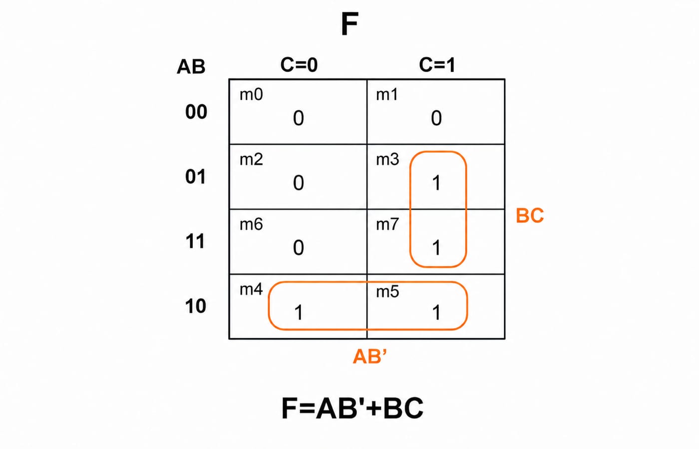
The output is 1 at minterms m(3,4,5,7). In a three-variable K-map, put rows AB in Gray order 00,01,11,10 and columns C=0,1. The row values are 00: 0,0; 01: 0,1; 11: 0,1; and 10: 1,1.
Group m4,m5 to obtain AB'. Group m3,m7 to obtain BC. There are no don't-care cells. These two groups independently produce F=AB'+BC, matching the circuit for every row. The circuit and reduced expression therefore agree on all eight inputs. Function Equivalence in Boolean Algebra handles the different task of proving that two independently presented functions match by a complete table, algebra, a K-map, or an XOR miter.
4. Worked Example 2: Decode a Four-NAND XOR Circuit
Do not jump from the diagram to a familiar symbol. Label all four NAND outputs first:
D = NAND(A,B)
E = NAND(A,D)
G = NAND(B,D)
Q = NAND(E,G)
Now propagate every possible input pair.
A | B | D | E | G | Q |
|---|---|---|---|---|---|
0 | 0 | 1 | 1 | 1 | 0 |
0 | 1 | 1 | 1 | 0 | 1 |
1 | 0 | 1 | 0 | 1 | 1 |
1 | 1 | 0 | 1 | 1 | 0 |
The algebra identifies the function:
E = (A.D)' = A' + D' = A' + AB = A' + B
G = (B.D)' = B' + D' = B' + AB = A + B'
Q = [(A' + B)(A + B')]' = A'B + AB' = A ⊕ B
For A=0, B=1, the internal values are D=1, E=1, G=0, Q=1. In contrast, for A=1, B=1, they are D=0, E=1, G=1, Q=0. Both the table and the algebra identify XOR.
5. Choose the Fastest Reliable Analysis Method
Use direct gate propagation when one input vector is supplied. For Example 1 at A=1, B=1, C=0, the whole solution is X=1, B'=0, Y=0, F=0. Expanding the expression would add work without adding confidence.
Use a truth table when there are only a few inputs and you need the whole function. Use Boolean algebra or a K-map when the task asks for a minimal expression or equivalent circuit. Larger tabular minimisation problems may call for the Quine-McCluskey method.
One convenient vector can disprove equivalence when the outputs differ, but it cannot prove equivalence. A complete truth table, valid Boolean identities, or a correctly grouped K-map can establish equivalence.
6. Common Traps and How to Catch Them
A NAND output is the complement of an AND output. In Example 2, A=B=1 makes D=0, not 1. OR and XOR also differ at 11: OR gives 1, while XOR gives 0. Write a value beside every inversion bubble and use the 11 row as a quick XOR diagnostic.
Reconvergent signals remain related. The B entering X=A+B and the B' entering Y=B'+C come from one input. They cannot be assigned separately. In the reduced result AB'+BC, B sends A through when B=0 and C through when B=1. Swapping the complemented and uncomplemented selector terms would reverse those cases.
For a K-map, check that rows follow Gray order 00,01,11,10, groups contain a power of two cells, and diagonal cells are not adjacent. Finally, test the simplified expression on rows where the output changes.
7. How Exams Turn the Same Circuit into Different Questions
The same network can support several question forms: find the output for a given vector, derive its Boolean expression, identify its truth table or named function, minimise its gate count, recognise a MUX-like or XOR-like rule, or translate an AND/OR circuit into NAND-only form.
Try this four-part checkpoint, then compare immediately:
Example 1 at
111givesX=1, Y=1, F=1.Example 1 at
110givesX=1, Y=0, F=0.The NAND network at
10givesQ=1.One inverter after
Qproduces XNOR, which is1for00and11.
For timed, exam-style work, use the GATE Test Series after you can reproduce the node equations without looking back.
8. The Short Version and the Next Step
Keep this five-line checklist beside the diagram:
Label every intermediate node.
Translate one gate at a time.
Propagate the supplied input values.
Simplify only after the expression is correct.
Verify with a second method.
The two patterns worth recognising are (A+B)(B'+C)=AB'+BC and the four-NAND implementation of A ⊕ B. Use the GATE category to place this topic in the wider preparation path.
Keep learning

Functional Completeness in Digital Logic: NAND, NOR and Worked Examples
Learn what makes a Boolean operator set complete, how NAND and NOR recover a standard basis, and how to verify a four-gate NAND construction.
Updated 2 Oct 20266 min readDigital Logic

Boolean Function Counts: Formulas, Worked Examples and Exam Traps
Build the master Boolean-function formula from output choices, then learn how common restrictions change the count through combinations, pairing and inclusion-exclusion.
Updated 27 Sep 20266 min readDigital Logic

Analog-Digital Conversion Basics: ADC, DAC, Worked Examples and Exam Patterns
Build ADC and DAC basics from one consistent transfer model, then practise code selection, reconstruction error, flash and SAR conversion, and bit-depth calculations.
Updated 25 Sep 20266 min readDigital Logic

Universal Realization with NAND and NOR Gates: Concepts, Worked Example and Exam Patterns
Learn why NAND and NOR are universal, then implement one three-variable function using four NAND gates and four NOR gates with verified input traces.
Updated 23 Sep 20265 min readDigital Logic