Combinational Circuits MCQs: 12 solved questions on MUX, decoders and adders
Combinational circuits MCQs with solutions: 12 solved GATE questions on multiplexers, decoders and ROMs, half and full adders, and carry-lookahead adders.
KnowledgeGate Team
Exam prep & CS education
17 Jul 20268 min read125 views
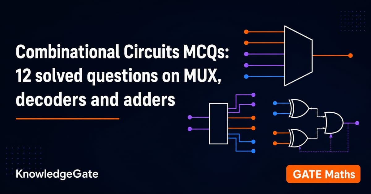
Combinational circuits are where Boolean algebra becomes hardware: multiplexers, decoders and encoders, adders, and the ROM-as-lookup-table trick. GATE tests these less as memorised block diagrams and more as sizing and delay problems, how big a MUX you need, how many decoders a memory expansion takes, how a carry-lookahead adder beats ripple carry. Every question below is a previous-year GATE problem, dated 1996 to 2016, and the sizing arguments have barely shifted across those twenty years, which is why the old papers still pay. Attempt each one before reading its answer, and follow the solution link when you want the full derivation. The Digital Electronics learn module carries the circuit theory behind them if you need to rebuild a block from scratch.
Multiplexers
Q1. A multiplexer with a 4-bit data select input is a (GATE 1998)
(a) 4:1 multiplexer
(b) 2:1 multiplexer
(c) 16:1 multiplexer
(d) 8:1 multiplexer
Answer: (c) 16:1 multiplexer. A MUX with n select lines chooses among 2^n data inputs, so 4 select lines address 2^4 = 16 inputs. The select-line count, not the data-input count, is what the phrase "4-bit data select" pins down. This one-line fact anchors every MUX-sizing question that follows (see the full MUX sizing solution).
Q2. A multiplexer has data inputs X and Y and control input Z, where Z = 0 selects X and Z = 1 selects Y. The connections that realize f = T + R with no extra hardware are (GATE 2004)
(a) R to X, 1 to Y, T to Z
(b) T to X, R to Y, T to Z
(c) T to X, R to Y, 0 to Z
(d) R to X, 0 to Y, T to Z
Answer: (a) R to X, 1 to Y, T to Z. The MUX output is X.Z′ + Y.Z. Feeding R to X, constant 1 to Y, and T to the select gives R.T′ + 1.T, which is RT′ + T, and that absorbs to T + R. Treating a 2:1 MUX as a tiny truth-table engine is the key idea behind implementing logic on multiplexers (see the full MUX logic solution).
Q3. If only one multiplexer and one inverter may be used to implement any Boolean function of n variables, the minimum MUX size needed is (GATE 2007)
(a) 2^n line to 1 line
(b) 2^(n+1) line to 1 line
(c) 2^(n-1) line to 1 line
(d) 2^(n-2) line to 1 line
Answer: (c) 2^(n-1) line to 1 line. Use n-1 of the variables as select lines, which leaves 2^(n-1) data inputs. Each data input must equal the function for that fixed select combination, and the remaining variable means each data line is one of 0, 1, the variable, or its complement, all reachable with a single inverter. That is why one inverter is exactly enough (see the full universal-MUX solution).
Decoders, ROMs and memory addressing
Q4. A RAM chip has capacity 1024 words of 8 bits each (1K x 8). The number of 2 x 4 decoders with an enable line needed to build a 16K x 16 RAM from these chips is (GATE 2013)
(a) 4
(b) 5
(c) 6
(d) 7
Answer: (b) 5. Doubling the word width to 16 bits just places chips in parallel and needs no extra selection, but the depth grows 16-fold, so you must generate 16 chip-select lines from 4 address bits. A tree of 2 x 4 decoders does this with one first-level decoder feeding the enables of four second-level decoders, giving 1 + 4 = 5. Width adds chips; only depth adds decoding (see the full memory expansion solution).
Q5. A ROM stores the full multiplication table of two 8-bit unsigned integers. The size of ROM required is (GATE 1996)
(a) 256 x 16
(b) 64K x 8
(c) 4K x 16
(d) 64K x 16
Answer: (d) 64K x 16. The two operands together form the address, so 8 + 8 = 16 address bits give 2^16 = 64K locations. The product of two 8-bit numbers can be up to 16 bits wide, so each location stores 16 bits. A lookup ROM is always sized as (2^address-bits) by (output width) (see the full ROM sizing solution).
Q6. The amount of ROM needed to implement a 4-bit multiplier is (GATE 2012)
(a) 64 bits
(b) 128 bits
(c) 1 Kbits
(d) 2 Kbits
Answer: (d) 2 Kbits. Two 4-bit operands make 8 address bits, so 2^8 = 256 entries. Their product needs up to 8 bits, so total storage is 256 x 8 = 2048 bits, that is 2 Kbits. This is the same address-by-width rule as Q5, scaled down (see the full ROM multiplier solution).
Adders and carry lookahead
Q7. The number of full adders and half adders required to add two 16-bit numbers is (GATE 1999)
(a) 8 half-adders, 8 full-adders
(b) 1 half-adder, 15 full-adders
(c) 16 half-adders, 0 full-adders
(d) 4 half-adders, 12 full-adders
Answer: (b) 1 half-adder, 15 full-adders. The least significant bit has no incoming carry, so a half adder suffices there. Every one of the remaining 15 positions must add three bits, the two operand bits plus the carry in, which is precisely a full adder. Ripple-carry adder sizing always follows this 1-plus-(n-1) pattern (see the full adder count solution).
Q8. For a carry-lookahead adder on two n-bit integers, built from gates of fan-in at most two, the time to perform the addition is (GATE 2016)
(a) Theta(1)
(b) Theta(log n)
(c) Theta(sqrt n)
(d) Theta(n)
Answer: (b) Theta(log n). The carries are computed by a parallel-prefix tree over the generate and propagate signals, and a balanced binary tree of two-input gates has depth logarithmic in n. That is the whole reason lookahead beats the linear Theta(n) of ripple carry. The fan-in-two constraint is what forces the log rather than a constant depth (see the full lookahead delay solution).
Q9. A 4-bit carry-lookahead adder is built from AND, OR, NOT, NAND, NOR gates, inputs available in both forms, each gate delay one unit, and the carry network in two-level AND-OR logic. Its overall propagation delay is (GATE 2004)
(a) 4 time units
(b) 6 time units
(c) 10 time units
(d) 12 time units
Answer: (b) 6 time units. Generating each propagate signal Pi = Ai XOR Bi takes two levels of AND-OR, so 2 units. The lookahead carry network is itself two-level AND-OR, adding 2 more. The final sum bit Si = Pi XOR Ci is again a two-level XOR, 2 units, for a total of 6. Contrast this fixed 6 with ripple carry, whose delay would grow with the word length (see the full CLA delay solution).
Q10. With Pi = Ai XOR Bi and Gi = Ai.Bi available, and AND/OR gates of any fan-in, the number of AND gates and OR gates needed for the 4-bit lookahead carry generator (outputs S3, S2, S1, S0 and C4) is (GATE 2007)
(a) 6, 3
(b) 10, 4
(c) 6, 4
(d) 10, 5
Answer: (b) 10, 4. Expand the carries in terms of G, P and C0: C1 has 1 product term, C2 has 2, C3 has 3 and C4 has 4, giving 1 + 2 + 3 + 4 = 10 AND gates. Each of the four carries C1 through C4 then needs one OR gate to sum its product terms, so 4 OR gates. Counting product terms per carry is the reliable way to size a lookahead generator (see the full carry generator solution).
Multipliers and combinational design
Q11. For an array multiplier of two n-bit numbers with unit-delay gates, the total delay is (GATE 2003)
(a) Theta(1)
(b) Theta(log n)
(c) Theta(n)
(d) Theta(n^2)
Answer: (c) Theta(n). Partial products are generated in parallel, but the critical path still ripples carries diagonally across the adder array, and that longest path spans a linear number of adder stages. It does not touch all n^2 cells, which is the trap in option (d). An array multiplier is linear in delay while using quadratic hardware (see the full array multiplier solution).
Q12. A circuit takes a decimal digit as 4 bits (0 as 0000 up to 9 as 1001) and outputs 1 when the digit is 5 or more. Using only AND, OR and NOT gates, the minimum number of gates required is (GATE 2004)
(a) 2
(b) 3
(c) 4
(d) 5
Answer: (b) 3. Label the bits A B C D from the 8s place down. The digits 5 to 9 are exactly those with A = 1, or with B = 1 and at least one of C or D set, so the output is A + B(C + D). That reads off as one OR for C + D, one AND for B(C + D), and one final OR, three gates in total (see the full gate minimisation solution).
How this set is examined
The 12 questions above map to the four pillars of combinational design: multiplexers as universal logic blocks (Q1 to Q3), decoders and ROM lookup tables for addressing and arithmetic (Q4 to Q6), adders from single bits up to carry-lookahead (Q7 to Q10), and multipliers plus custom logic design (Q11 to Q12). The through-line is sizing and delay: almost every question is really asking how many blocks, how many gates, or how deep the critical path. That framing carries into the Sequential circuits MCQs, where feedback and clocking are added on top.
If a block still feels shaky, the full theory with worked circuits sits in our Combinational circuits: multiplexers, decoders and adders deep dive. GATE aspirants get the full digital electronics sequence inside GATE Guidance by Sanchit Sir, and you can place the subject in the wider syllabus on the GATE CS Exam page. Solve, review the ones you missed, and come back a week later; the second pass is where the marks get locked in.
Keep learning
Special Logic Circuits MCQs: 12 Solved Questions on Adders, Encoders, PLA and DAC
Solve 12 special logic circuits MCQs covering recognition, hardware counts, Boolean identities and numerical calculations. Each answer includes the reasoning you should reproduce in an exam.
19 Sep 20268 min read64 viewsDigital Electronics MCQs
Function Equivalence MCQs: 12 Solved Boolean Algebra Problems
Solve 12 function-equivalence questions step by step, from De Morgan's law and absorption to minterm sets, counterexamples and a four-option MSQ.
Updated 17 Sep 20268 min readDigital Electronics MCQs

CLA & Arithmetic Logic MCQs: 10 Solved Questions with Explanations
Solve ten CLA and arithmetic logic MCQs with compact workings for carry equations, timing paths, hardware sizing and operand-pair counting.
Updated 16 Sep 20267 min readDigital Electronics MCQs
Sync Counter Design MCQs: 11 Solved Questions on Modulus, State Sequences and Excitation Logic
Solve 11 synchronous-counter questions covering modulus boundaries, repeated outputs, common-clock tracing, excitation equations, enables and composite states.
Updated 14 Sep 20267 min readDigital Electronics MCQs