Shift Registers MCQs: 10 Solved Questions on Timing, Modes and LFSRs
Solve ten published shift-register questions covering circuit recognition, serial and parallel transfer, timing calculations, and XOR-feedback traces.
KnowledgeGate Team
Exam prep & CS education
9 Sep 20267 min read
Shift-register definitions can feel easy until one question mixes a timing formula with serial movement, or an LFSR asks for the state several clocks later. Circuit recognition and loading modes lead into numerical timing and feedback-state tracing. Attempt each item before reading its explanation, and write the state after every clock in feedback-register questions. More than 10 Shift Registers practice questions are available on KnowledgeGate. For adjacent practice on the storage elements behind registers, use Sequential Circuits MCQs: 11 Solved Flip-Flops for flip-flop and counter behaviour; use the register questions below for loading modes, timing and feedback states.
Related reading: Shift register types and Flip-flops.
1. Shift Registers MCQs on circuit type, loading and data movement
Stored state, loading, and data movement are key shift-register concepts.
Q1. A register is a sequential circuit
PYQ: TPSC System Analyst 2026
Which of the following is a SEQUENTIAL circuit ?
A.
PARITYB.
ADDERC.
REGISTERD.
MULTIPLEXER
Correct answer: C. REGISTER
A register contains memory elements, so its output depends on stored state and current input. The other three circuits normally depend only on current inputs. Memory is the deciding test.
Open Q1 in the Shift Registers module.
Q2. Identify the PIPO diagram
PYQ: DSSSB TGT 2023
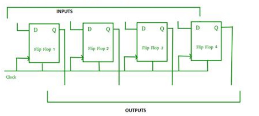
The given diagram expresses ______.
A.
Parallel-In Parallel-Out Shift RegisterB.
Serial-In Parallel-Out Shift RegisterC.
Serial-In Serial-Out Shift RegisterD.
Parallel-In Serial-Out Shift Register
Correct answer: A. Parallel-In Parallel-Out Shift Register
Several input lines feed the stages, and every stage output is exposed, so bits enter and leave together. This is parallel-in, parallel-out. SIPO has serial entry, while PISO has serial exit.
Open Q2 in the Shift Registers module.
Q3. Synchronous parallel loading takes one pulse
PYQ: KVS 2018
To load a byte of data parallelly into a shift register with a synchronous load, there must be _____.
A.
one clock pulseB.
one clock pulse for each 1 in the dataC.
eight clock pulsesD.
one clock pulse for each 0 in the data
Correct answer: A. one clock pulse
A synchronous parallel load captures all eight bits on the same active edge. One pulse therefore loads the byte. Eight pulses describe serial loading, with one bit entering per pulse.
Open Q3 in the Shift Registers module.
Q4. Reading several bytes through a shift register
PYQ: BPSC NB 2024
In order to read multiple bytes of a row at the same time, we make use of ______.
A.
Memory extensionB.
LatchC.
Shift registerD.
More than one of the aboveE.
None of the above
Correct answer: C. Shift register
A shift register can accept a stream over successive clocks and expose its stored bits together, or perform the reverse conversion. A latch stores a value without controlled shifting. Memory extension changes capacity, not transfer mode.
Open Q4 in the Shift Registers module.
2. Shift register timing MCQs with complete clock calculations
Use T = 1/f. Under the SISO loading-plus-reading convention, total clocks are 2N - 1.
Q5. Delay through an 8-bit register at 400 MHz
PYQ: ISRO 2023
The time delay obtained through an 8-bit serial register with 400 MHz clock is:
A.
20 nsB.
2.5 µsC.
20 µsD.
2.5 µs
Correct answer: A. 20 ns
T = 1/f = 1/(400 × 10^6) s = 2.5 × 10^-9 s = 2.5 ns
Delay = 8T = 8 × 2.5 ns = 20 ns
Here 2.5 ns is one clock period, not the delay through eight stages. The duplicated 2.5 µs choices appear twice in the printed options.
Open Q5 in the Shift Registers module.
Q6. Loading and reading 32 bits in SISO mode
Consider a 32- bit shift register which uses a clock of 1 GHz. If register is operated in SISO mode, find total time required to perform loading and reading?
A.
1 nsB.
31 nsC.
32 nsD.
63 ns
Correct answer: D. 63 ns
T = 1/(1 × 10^9) s = 1 × 10^-9 s = 1 ns
Loading takes 32 pulses. Once the first output bit appears, the remaining 31 bits need 31 more pulses, so total time = (32 + 31) × 1 ns = (2 × 32 - 1) × 1 ns = 63 ns.
Practise Q6 from the module hub.
3. LFSR MCQs solved by tracing every register state
Write every post-clock LFSR state, follow the shown shift direction, and apply XOR before insertion. Review Sequential Circuits: Flip-Flops and Counters if the flip-flop transitions need a refresh.
Q7. Six input bits through a four-bit LFSR
PYQ: GATE Information Technology 2007
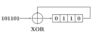
What is the final value stored in the linear feedback shift register if the input is 101101?
A.
0110B.
1011C.
1101D.
1111
Correct answer: A. 0110
Begin at 0000, shift left, and insert input XOR old rightmost bit on the right. Inputs 1 0 1 1 0 1 give 0001 → 0011 → 0110 → 1101 → 1011 → 0110. The final content is 0110; 1101 and 1011 are intermediate states.
Open Q7 in the Shift Registers module.
Q8. Run an XOR-feedback register four clocks backward
Consider the following circuit with present state Q0=Q1=0 and Q2=Q3=1.
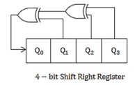
What was the state of the register before 4 clock cycles?
A.
Q0 = 0, Q1 = 1, Q2 = 0, Q3 = 0B.
Q0 = 1, Q1 = 0, Q2 = 1, Q3 = 0C.
Q0 = 1, Q1 = 0, Q2 = 0, Q3 = 0D.
None
Correct answer: A. Q0 = 0, Q1 = 1, Q2 = 0, Q3 = 0
Read states in Q0Q1Q2Q3 order and invert the shown XOR-feedback relation. From 0011, step backward through 0110 → 1101 → 1010 → 0100. Thus Q0=0, Q1=1, Q2=0, Q3=0; forward replay gives 0100 → 1010 → 1101 → 0110 → 0011.
Practise Q8 in the Shift Registers section.
4. Feedback shift register MCQs with nine-clock and three-clock traces
These longer traces are safest when every intermediate state is visible.
Q9. Three-bit XOR register after nine input bits
PYQ: GATE 2006
Consider the circuit in the diagram. The ⊕ operator represents Ex-OR. The D flipflops are initialized to zeroes (cleared).
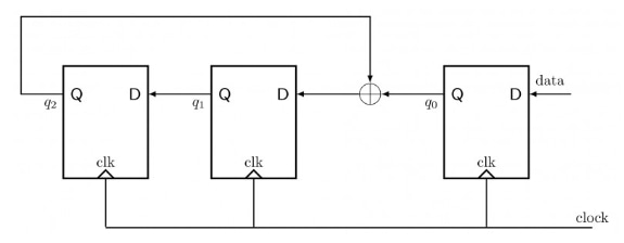
The following data: 100110000 is supplied to the “data” terminal in nine clock cycles. After that the values of q2q1q0 are:
A.
000B.
001C.
010D.
101
Correct answer: C. 010
Starting at q2q1q0 = 000, apply q2(new)=q1(old), q1(new)=q0(old) and q0(new)=data XOR q2(old). Inputs 1 0 0 1 1 0 0 0 0 produce 001 → 010 → 100 → 000 → 001 → 010 → 100 → 001 → 010. The ninth-clock state is therefore 010.
Open Q9 in the Shift Registers module.
Q10. Five-bit reducer after three clocks
Consider 5-bit left shift reducer and D flip flop shown in figure below:
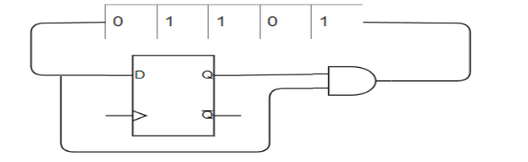
The bits present in queue after 3 clocks:
A.
01010B.
01110C.
01011D.
10110
Correct answer: C. 01011
Follow the shift and recirculating D-input connection exactly as drawn. Starting from the figure's 01101, the clock-by-clock states are 01101 → 11010 → 10101 → 01011. After three clocks the register contains 01011; choosing 10110 means the direction or bit order was reversed.
Practise Q10 in the Shift Registers section.
5. Shift register mistakes that turn correct arithmetic into a wrong option
Trap | Wrong move | Check |
|---|---|---|
Eight-stage delay | Use | Calculate |
SISO loading and reading | Use | Use |
Parallel loading | Count eight pulses | Load all bits on one edge |
Shift direction | Reverse left and right | Mark direction before tracing |
LFSR final state | Report intermediate | Finish at |
For clock-by-clock practice, use Sync Counter Analysis MCQs.
6. Common shift-register question types
Shift-register questions commonly test circuit-class identification, clock-pulse counting, frequency-to-time conversion, and XOR-feedback state tracing. A PYQ label identifies the cited exam and year; it does not establish topic frequency or weightage. Use the same three-step order each time: mark shift direction and state order, write one update rule, then complete the full timing or state table on paper before checking the options.
7. Shift registers MCQs: the short version and next step
Memory distinguishes a register from combinational logic. Parallel load takes one active edge, timing begins with T = 1/f, and feedback questions require a written state after every clock. For a structured route from the basics through Digital Electronics and the wider syllabus, see GATE Guidance by Sanchit Sir. To compare the broader preparation catalogue, use GATE CS Exam Preparation.
Keep learning
Special Logic Circuits MCQs: 12 Solved Questions on Adders, Encoders, PLA and DAC
Solve 12 special logic circuits MCQs covering recognition, hardware counts, Boolean identities and numerical calculations. Each answer includes the reasoning you should reproduce in an exam.
19 Sep 20268 min readDigital Electronics MCQs
Function Equivalence MCQs: 12 Solved Boolean Algebra Problems
Solve 12 function-equivalence questions step by step, from De Morgan's law and absorption to minterm sets, counterexamples and a four-option MSQ.
Updated 17 Sep 20268 min readDigital Electronics MCQs

CLA & Arithmetic Logic MCQs: 10 Solved Questions with Explanations
Solve ten CLA and arithmetic logic MCQs with compact workings for carry equations, timing paths, hardware sizing and operand-pair counting.
Updated 16 Sep 20267 min readDigital Electronics MCQs
Sync Counter Design MCQs: 11 Solved Questions on Modulus, State Sequences and Excitation Logic
Solve 11 synchronous-counter questions covering modulus boundaries, repeated outputs, common-clock tracing, excitation equations, enables and composite states.
Updated 14 Sep 20267 min readDigital Electronics MCQs