

Universal Shift Register: Modes, Circuit and Worked Timing Example
Follow a four-bit universal shift register through loading, right shift, left shift and hold. See how four multiplexers select the next state, then practise tracing bits at each rising clock edge.
KnowledgeGate Team
Exam prep & CS education
Updated 6 Nov 20265 min read

Remembering four mode names does not tell you which bit enters a universal shift register, which bit leaves, or when its outputs change. The difficulty is keeping direction, input selection and clock timing consistent while the mode changes. A four-bit circuit and an original clock-by-clock example keep the bit order explicit: Q3 Q2 Q1 Q0 order, with the MSB on the left.
What makes a shift register universal?
A four-bit universal shift register uses four flip-flops to store four bits. Its selection inputs choose among four operations: hold the current word, shift right, shift left, or load a new word in parallel. Here we use D flip-flops, which store their selected D inputs at the active clock edge.
“Universal” refers to these transfer choices. It does not mean unlimited storage or arbitrary arithmetic. A register that shifts in both directions need not also provide parallel loading and hold.
Serial transfer admits one new bit per active edge. Parallel loading stores all four input bits at one edge. For the SISO, SIPO, PISO and PIPO background, read shift-register types and timing. Ring and Johnson counters use feedback to sequence states; their counter-specific treatment is in ring and Johnson counter state cycles. This post focuses on four-mode selection and timing.
Fix the mode table and bit-direction convention
The following convention fixes the labels for the tables and trace; a question or device datasheet can define different labels. All operations occur on rising clock edges, inputs meet setup and hold requirements, and reset stays inactive throughout the trace.
SR is the serial bit entering Q3 during right shift. SL enters Q0 during left shift. P3 through P0 are parallel data inputs, distinct from the flip-flops' D inputs.
S1 S0 | Operation | Next Q3 Q2 Q1 Q0 |
|---|---|---|
00 | Hold | Q3 Q2 Q1 Q0 |
01 | Right shift | SR Q3 Q2 Q1 |
10 | Left shift | Q2 Q1 Q0 SL |
11 | Parallel load | P3 P2 P1 P0 |
Every Q on the right denotes the old state. All next-state bits update together. Parallel inputs are irrelevant during shift and hold; unused serial inputs are don't-cares.
Texas Instruments' CD74HC194 documentation distinguishes synchronous parallel loading from a separate asynchronous master reset. That is a device-specific reset arrangement, not a fifth selection in our two-bit mode table.
How four multiplexers choose the next state
Place one 4:1 multiplexer before each D flip-flop. All four MUXes share S1 and S0, and all flip-flops share a clock. MUX inputs I0, I1, I2 and I3 correspond to modes 00, 01, 10 and 11 respectively.
Flip-flop input | I0: hold | I1: right | I2: left | I3: load |
|---|---|---|---|---|
D3 | Q3 | SR | Q2 | P3 |
D2 | Q2 | Q3 | Q1 | P2 |
D1 | Q1 | Q2 | Q0 | P1 |
D0 | Q0 | Q1 | SL | P0 |
Check the internal stages with old Q=1011 and mode 01: D2=old Q3=1, while D1=old Q2=0. With SR=0, the complete D word is 0101. The next rising edge stores it.
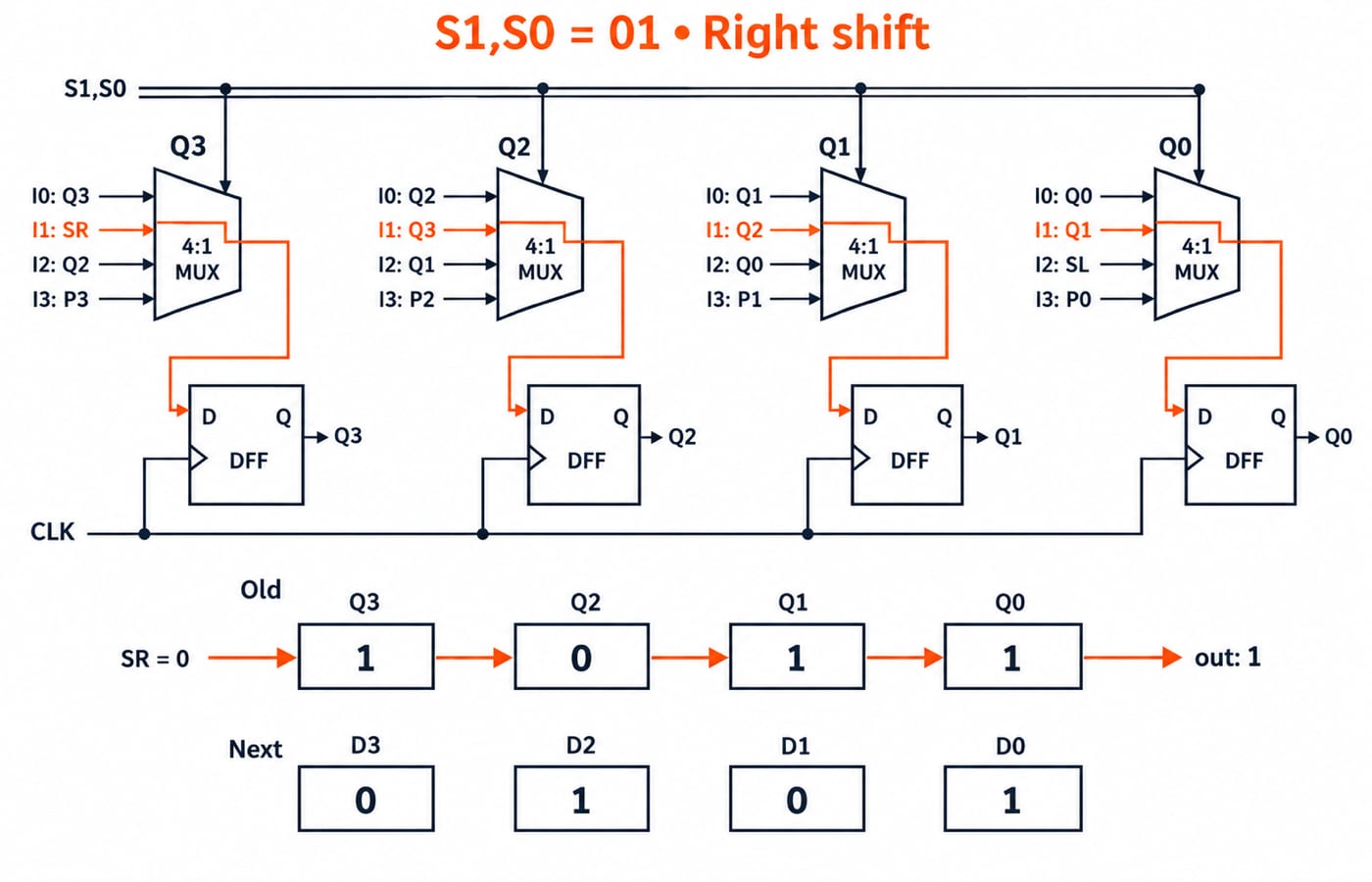
Hold selects each flip-flop's own Q feedback. Continued clocking therefore preserves the word; this circuit does not need clock gating for hold. If selecting these paths feels unclear, revise multiplexer selection logic.
Worked timing example: load, shift both ways and hold
The initial state is given as 0000 before edge 1. We are not assuming that an unreset device powers up to zero. Use a teaching clock period of 10 ns, with rising edges at 10, 20, 30, 40, 50 and 60 ns.
Inputs settle before each relevant edge. Ignore propagation delay for this idealised trace; input changes between edges do not directly change Q while reset is inactive.
Edge/time | S1S0 | Relevant input | Before | After | Discarded bit |
|---|---|---|---|---|---|
1 / 10 ns | 11 | P=1011 | 0000 | 1011 | n/a |
2 / 20 ns | 01 | SR=0 | 1011 | 0101 | old Q0=1 |
3 / 30 ns | 01 | SR=1 | 0101 | 1010 | old Q0=1 |
4 / 40 ns | 10 | SL=1 | 1010 | 0101 | old Q3=1 |
5 / 50 ns | 00 | P=1111, ignored | 0101 | 0101 | n/a |
6 / 60 ns | 11 | P=0110 | 0101 | 0110 | n/a |
At edge 2, use the old word 1011. New Q3 receives SR=0; new Q2 receives old Q3=1; new Q1 receives old Q2=0; new Q0 receives old Q1=1. Together they form 0101, and old Q0=1 leaves the stored word.
At edge 3, prefix SR=1 to the old upper three bits 010, giving 1010. At edge 4, shift that word left: new Q3=old Q2=0, new Q2=old Q1=1, new Q1=old Q0=0, and new Q0=SL=1. The result is 0101; old Q3=1 is discarded.
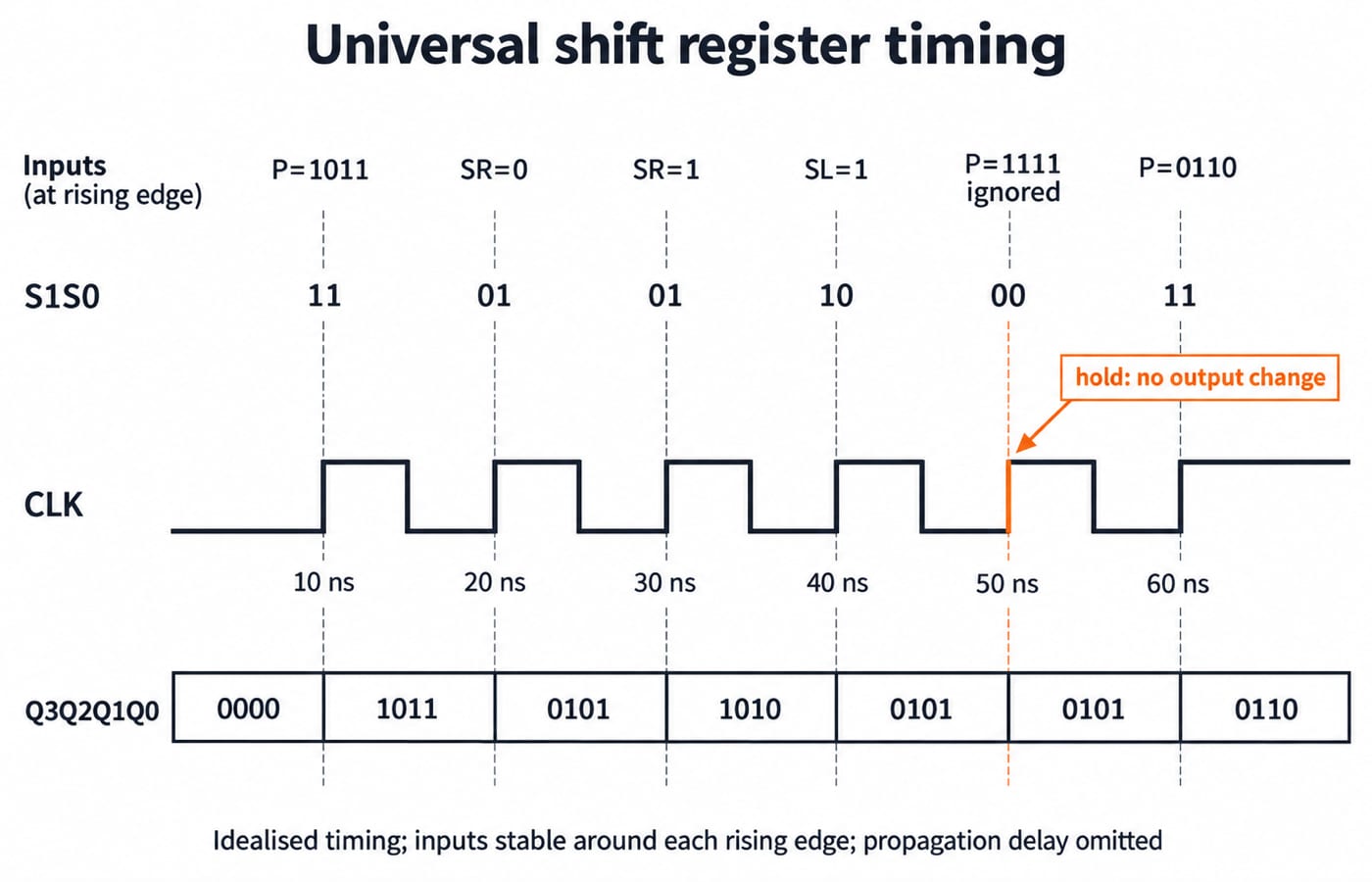
At edge 5, mode 00 selects feedback, so P=1111 is ignored. Only edge 6 selects parallel data again. “Discarded bit” means the old boundary bit lost from storage during shifting, not a bit captured by an extra latch.
Three traps that change the answer
Direction ambiguity: drawn arrows are insufficient without bit significance. Write the next-state vector first. From 1011 with zero fill, right shift gives 0101, whereas left shift gives 0110. Our MSB stays on the left of every printed word.
In-place updating: copying an already-updated bit into another position models sequential software assignments, not simultaneous flip-flop sampling. Keep separate old and new rows, as at edge 2. Also, parallel load waits for the active edge; Q does not immediately follow P when mode 11 is selected.
Arithmetic assumptions: arbitrary serial inputs are neither automatic zero fill nor automatic sign extension. For unsigned values, 1011 is 8+2+1=11. Zero-fill right shift gives 0101, or 4+1=5. Zero-fill left shift gives 0110, or 4+2=6: doubling gives 22, but four-bit truncation leaves 22-16=6. The original MSB is lost. Rotation requires explicitly feeding the outgoing bit into the incoming position.
How to approach GATE-style register questions
IIT Guwahati's GATE 2026 CS syllabus lists combinational and sequential circuits in Section 2, Digital Logic. The worked trace applies those topics to a universal register; it is neither an official prediction nor a past-paper question. For broader preparation options, see GATE preparation courses and test series.
Try this original self-check. Start with Q=1100. Edge A uses mode 01 with SR=1; edge B uses mode 10 with SL=0; edge C uses mode 00. Find the final word and the boundary bits discarded at A and B.
At A, prepend 1 to old Q3Q2Q1=110: 1110, discarding old Q0=0. At B, append 0 to old Q2Q1Q0=110: 1100, discarding old Q3=1. C holds 1100.
Solve in this order: record bit order and active edge, decode the mode, select its relevant input, then compute every new bit from the old row. Do not count falling edges in this rising-edge circuit.
Short version and next practice step
The mode lines choose each next-state source, and the active clock edge stores the selected word. Define the incoming serial bit before shifting.
Redo the main trace with SR at edge 3 changed to 0. Your check: edge 3 becomes 0010; edge 4 becomes 0101; edge 5 remains 0101; edge 6 loads 0110.
For an optional structured preparation next step, explore GATE Guidance by Sanchit Sir and decide whether it suits your wider study plan.
Go deeper with the full courseDigital Electronics
Keep learning
Shift Registers MCQs: 10 Solved Questions on Timing, Modes and LFSRs
Solve ten published shift-register questions covering circuit recognition, serial and parallel transfer, timing calculations, and XOR-feedback traces.
Updated 30 Oct 20267 min read72 viewsDigital Electronics MCQs
Shift Registers Explained: Types, Timing and a 4-Bit Worked Trace
Learn one reliable method for tracing shift registers. Fix the bit order, apply simultaneous next-state equations, and follow a complete four-clock example.
Updated 4 Sep 20266 min read92 viewsDigital Logic

Shift Registers, Ring and Johnson Counters for GATE: Frequency Division and Timing Numericals Solved
Build a 4-bit ring counter and Johnson counter state by state, then use their mod values to solve frequency-division and maximum-clock questions.
Updated 29 Jul 20265 min read60 viewsDigital Logic

ISRO CS COA Numericals: Cache Mapping, Pipeline Timing and Addressing Modes
Three reusable COA scratchpads turn cache mapping, pipeline penalties and signed addressing-mode displacements into quick, checkable calculations.
Updated 18 Nov 20266 min readComputer Organization & Architecture