Sequential circuits: flip-flops, latches and counters explained
Sequential circuits for GATE: SR, D, JK and T flip-flops, excitation tables, latch versus flip-flop, and a fully worked synchronous counter design example.
KnowledgeGate Team
Exam prep & CS education
Updated 15 Jul 20265 min read61 views
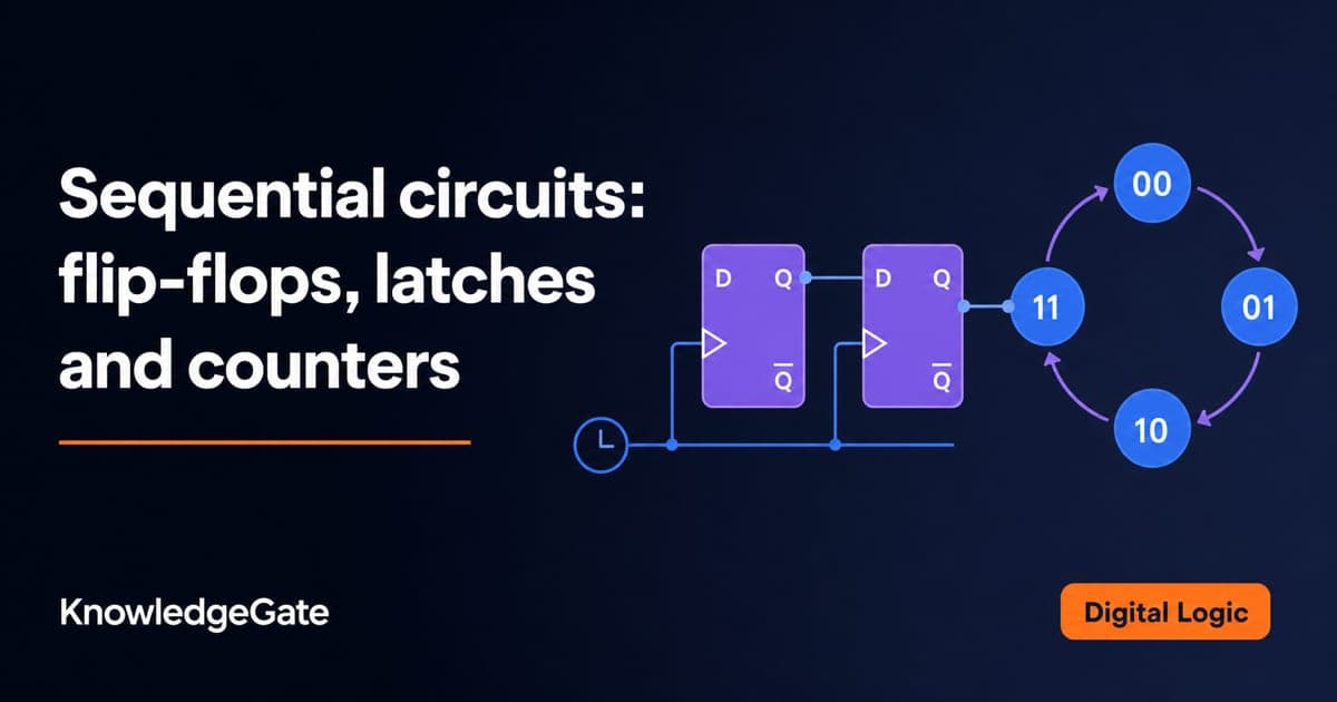
A sequential circuit remembers. Unlike a combinational circuit, its output depends on the present input and on the stored state, so the same input can give different outputs depending on history. That memory is built from flip-flops, and once you can read a flip-flop's characteristic and excitation tables you can design any synchronous counter to order. Marks are usually lost not on the definitions but on the two things built on top of them: which device is edge-triggered and which is merely transparent, and how to work backwards from a wanted count sequence to the inputs that produce it.
What makes a circuit sequential
A combinational circuit is a pure function of its current inputs, which is the whole subject of Combinational circuits: multiplexers, decoders and adders. A sequential circuit adds a feedback path and a memory element, so its behaviour depends on state as well as input. Synchronous sequential circuits update that state only on a clock edge, which keeps the whole system marching in step and makes timing analysable. Almost everything GATE tests here (counters, registers, sequence detectors) is synchronous, so assume a clock unless told otherwise.
Latch versus flip-flop: the timing distinction
This is the distinction examiners probe most. A latch is level-sensitive: it is transparent whenever its enable is at the active level, so the output follows the input for the entire time the enable is high. A flip-flop is edge-triggered: it samples its input only at the instant of a clock edge, rising or falling, and holds that value until the next edge. Edge triggering is what prevents a value from rippling uncontrollably through cascaded stages within one clock period, which is why registers and counters are built from flip-flops, not bare latches. A master-slave arrangement of two latches is the classic way to turn level sensitivity into edge behaviour.
The four flip-flops and their characteristic tables
Each flip-flop is defined by how its next state Q(t+1) depends on its inputs and present state Q(t). That forward map is its characteristic table, and the four standard devices differ only in what they do with the input combinations.
Flip-flop | Inputs to Q(t+1) | Characteristic equation |
|---|---|---|
SR (S R) | 00 holds, 01 resets to 0, 10 sets to 1, 11 is invalid | Q(t+1) = S + R'Q, valid only while SR = 0 |
JK (J K) | 00 holds, 01 resets, 10 sets, 11 toggles | Q(t+1) = JQ' + K'Q |
D | 0 stores 0, 1 stores 1 | Q(t+1) = D |
T | 0 holds, 1 toggles | Q(t+1) = T XOR Q |
SR flip-flop. Set and Reset inputs, the oldest of the four. The 1,1 combination is outlawed rather than defined, because it commands the device to set and reset at the same instant.
D flip-flop. One data input, and no way to misuse it. It stores whatever D was at the clock edge, which makes it the natural building block for registers.
JK flip-flop. The SR flip-flop with the forbidden state repaired: 1,1 is redefined as a toggle instead of being outlawed, which is why JK is the general-purpose choice in design questions.
T flip-flop. One toggle input. It is a JK with J and K tied together, and it is the workhorse of counters, since a counter bit is precisely a bit that flips on cue.
Excitation tables: designing backwards
A characteristic table answers "given the inputs, what is the next state". Design needs the reverse question: "given the state I have and the state I want, what inputs do I apply". That reverse map is the excitation table, and it is the single most useful tool in counter design.
Q(t) to Q(t+1) | SR (S R) | JK (J K) | D | T |
|---|---|---|---|---|
0 to 0 | 0 X | 0 X | 0 | 0 |
0 to 1 | 1 0 | 1 X | 1 | 1 |
1 to 0 | 0 1 | X 1 | 0 | 1 |
1 to 1 | X 0 | X 0 | 1 | 0 |
The X entries are don't-cares, and they are a gift: they give you freedom that shrinks the logic when you minimise with a K-map. The JK excitation table is especially loose, which is why JK-based designs often need the fewest gates.
A worked synchronous counter: state table to logic
Design a 2-bit synchronous counter that counts 0, 1, 2, 3, 0 using JK flip-flops. Call the state bits Q1 (high) and Q0 (low). First write the state table with the required present-to-next transitions, then read the flip-flop inputs from the JK excitation table above.
Present Q1 Q0 | Next Q1 Q0 | J1 K1 | J0 K0 |
|---|---|---|---|
0 0 | 0 1 | 0 X | 1 X |
0 1 | 1 0 | 1 X | X 1 |
1 0 | 1 1 | X 0 | 1 X |
1 1 | 0 0 | X 1 | X 1 |
Now minimise each input as a function of Q1 and Q0, using the don't-cares. For the low bit, J0 and K0 are 1 or don't-care in every row, so J0 = 1 and K0 = 1: the low flip-flop toggles every clock, which is exactly what a counter's least significant bit should do. For the high bit, the J1 column is defined only in the two rows where Q1 = 0, and there it equals Q0, so J1 = Q0; the K1 column is defined only in the two rows where Q1 = 1, and there it also equals Q0, so K1 = Q0. So the whole counter is J0 = K0 = 1, J1 = K1 = Q0.
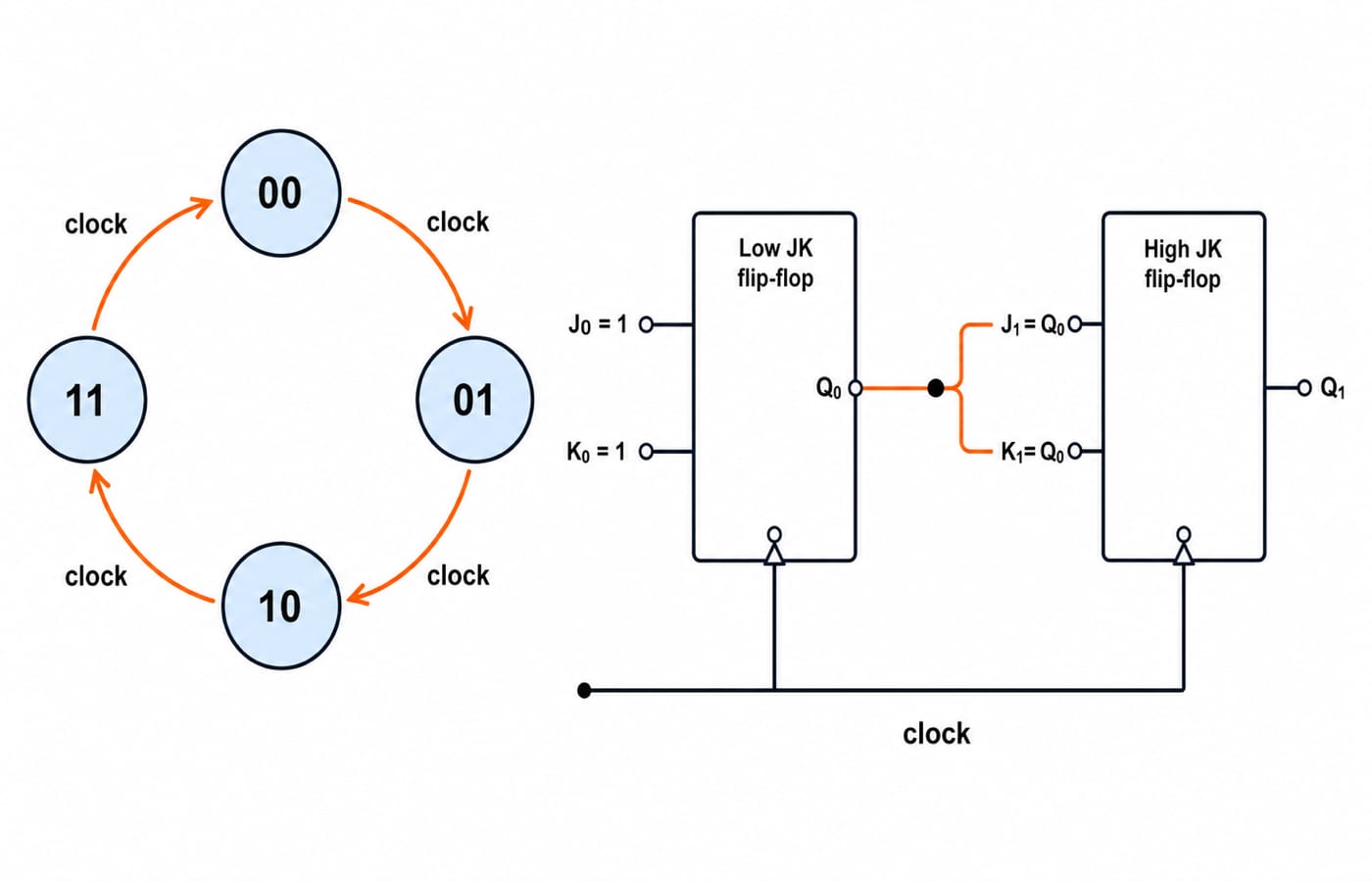
Trace it from 01: J1 = Q0 = 1 and K1 = 1, so Q1 toggles 0 to 1; J0 = K0 = 1, so Q0 toggles 1 to 0. The next state is 10, which is decimal 2, exactly the count we wanted. That procedure (state table, excitation lookup, K-map minimisation) designs any synchronous counter, not just this one.
How sequential circuits are tested in GATE
Sequential circuits is one of the denser slices of digital electronics: over 220 questions sit on the Sequential Circuits learn module, inside a digital electronics pool of more than 1,500. The steady patterns are: converting one flip-flop into another (make a T from a D, or a D from a JK), analysing a given counter to find its count sequence and modulus, a "number of flip-flops needed for a mod-N counter" question (the answer is the smallest n with 2^n at least N), and a latch-versus-flip-flop conceptual question. The counter-design question above is the constructive version they ask when they want a longer problem.
The recurring mistakes are forgetting the invalid SR state, misreading the JK excitation don't-cares as fixed values, and confusing level-triggered latch behaviour with edge-triggered flip-flop behaviour in a timing question. All three are conceptual, and a few hand-designed counters fix them for good.
The short version
Learn the four flip-flops by their next-state rule, memorise the JK excitation table, and practise the state-table-to-logic procedure until a counter design is routine. See where the topic sits among the rest of the syllabus on the Digital Electronics learn hub. For the full GATE build-up, from combinational into sequential design, GATE Guidance by Sanchit Sir sequences it the way the syllabus intends, with the CS Fundamentals category holding the supporting material.
Keep learning
NOT, OR and AND Gates: Evolution, Truth Tables and a Worked Circuit
Learn how NOT, OR and AND gates developed from switching ideas, then trace F=(A+B')C node by node and confirm it with a complete truth table.
Updated 23 Oct 20265 min readDigital Logic
Binary Arithmetic Operations Explained: Rules and Worked Examples
Learn binary addition, subtraction, multiplication and division with aligned worked examples, then separate carry, borrow and two's-complement overflow.
Updated 19 Oct 20266 min readDigital Logic
1's Complement Explained: Binary Conversion, Addition and Worked Examples
Learn how fixed-width 1's complement numbers represent negatives, why zero has two encodings, and how end-around carry works through exact examples.
Updated 15 Oct 20266 min readDigital Logic
Decimal Conversion Explained: Binary, Octal and Hexadecimal Worked Examples
Learn one dependable method for converting values between decimal, binary, octal and hexadecimal, including fractions, shortcuts and checks.
Updated 11 Oct 20265 min readDigital Logic