Hazards and Timing Questions: 10 Solved MCQs, NATs and Timing Problems
Ten solved Hazards and Timing questions with worked explanations for hazard types, consensus terms, K-map transitions, glitch duration and timing waveforms.
KnowledgeGate Team
Exam prep & CS education
Updated 29 Jul 20268 min read

A hazard is not a Boolean-function error: the steady-state result can be correct while unequal propagation delays produce a short false pulse. An exam may test a definition, consensus term, K-map transition, glitch width or waveform count.
Ten questions follow, grouped by what they test: two on definitions, two on consensus terms and fault counting, two K-map hazard hunts, two glitch-width calculations and two timing traces. Attempt each before reading its answer. Four of them open at the exact question inside the Hazards & Timing learn module, and the rest open the module itself, which carries the whole set.
1. Hazards and timing: build the decision rules before solving
Question signal | Meaning | Test |
|---|---|---|
Static-1 hazard | An intended | Check adjacent 1-minterms in a two-level SOP |
Static-0 hazard | An intended | Check adjacent 0-cells in a two-level POS |
Dynamic hazard | One intended transition toggles more than once before settling | Trace all unequal-delay, multi-level paths |
Essential hazard | Unequal feedback-path delays in asynchronous sequential logic | Trace the feedback loop and state changes |
Reconvergent paths with different propagation delays cause hazards. In a two-level SOP, adjacent 1-minterms covered by separate implicants need a common implicant. Add the consensus term to keep one product true throughout the transition. The Boolean Algebra and K-map Minimization Guide develops this grouping logic.
Glitch width is always the same subtraction. In Question 7 one path takes 6 + 10 = 16 ns and the other 11 ns, so the two arrivals disagree for |16 - 11| = 5 ns. That difference is the pulse width only when the inputs actually drive both paths.
2. Dynamic, static and essential hazard concept questions
Question 1: where the dynamic hazard problem occurs
ISRO 2016
The dynamic hazard problem occurs in
(a) combinational circuit alone
(b) sequential circuit only
(c) Both (a) and (b)
(d) None of the above
Answer: (c) Both (a) and (b). Practise the ISRO 2016 original
Unequal-delay, multi-level paths can occur in combinational logic or inside a sequential circuit. A dynamic hazard toggles repeatedly before settling. An essential hazard instead concerns unequal delays around asynchronous sequential feedback.
Question 2: define and distinguish the hazard family
Define what a hazard means in digital logic circuits and explain its primary root cause. Distinguish clearly between Static Hazards, Dynamic Hazards, and Essential Hazards, outlining how these unwanted glitches impact digital systems.
Answer: A hazard is a temporary pulse despite a correct steady-state result, usually caused by unequal delays along reconvergent paths. Static-1 follows 1 -> 0 -> 1; static-0 follows 0 -> 1 -> 0. Dynamic means multiple toggles during one intended transition. Essential belongs to asynchronous sequential feedback.
A glitch can clock a flip-flop, increment a counter or push an asynchronous machine into the wrong state. Synchronous sampling hides it only when the signal settles before the active clock edge.
3. Consensus terms and stuck-at fault counting
Question 3: add the consensus term that removes the hazard
Which of the following remove hazards from f(x,y,z) = x y +z x’?
(a) zx’+ xyz
(b) xy + x’z +yz
(c) xy + zx’
(d) xy + zx’+xz
Answer: (b) xy + x'z + yz.
Write xy + x'z. With y = z = 1, an x transition can turn both products off because x appears in opposite forms. Consensus term yz gives xy + x'z + yz without changing the function.
Question 4: count all multiple stuck-at faults
GATE 2005
A line L in a circuit is said to have a stuck-at-0 fault if the line permanently has a logic value 0. Similarly a line L in a circuit is said to have a stuck-at-1 fault if the line permanently has a logic value 1. A circuit is said to have a multiple stuck-at fault if one or more lines have stuck at faults. The total number of distinct multiple stuck-at faults possible in a circuit with N lines is
(a) 3^N
(b) 3^N - 1
(c) 2^N - 1
(d) 2
Answer: (b) 3^N - 1. Practise the GATE 2005 original
Each line is healthy, stuck at 0 or stuck at 1, giving 3^N assignments. Exclude all-healthy: 3^N - 1. For N = 2, the eight faults are (SA0, healthy), (SA1, healthy), (healthy, SA0), (healthy, SA1) and the four two-line stuck combinations. Stuck-at faults are a fault model, not a timing hazard: the line is permanently wrong rather than briefly wrong.
4. Static-1 hazards from K-maps and minterm transitions
Question 5: prove that a minimal SOP has no static-1 hazard
Consider the Boolean function
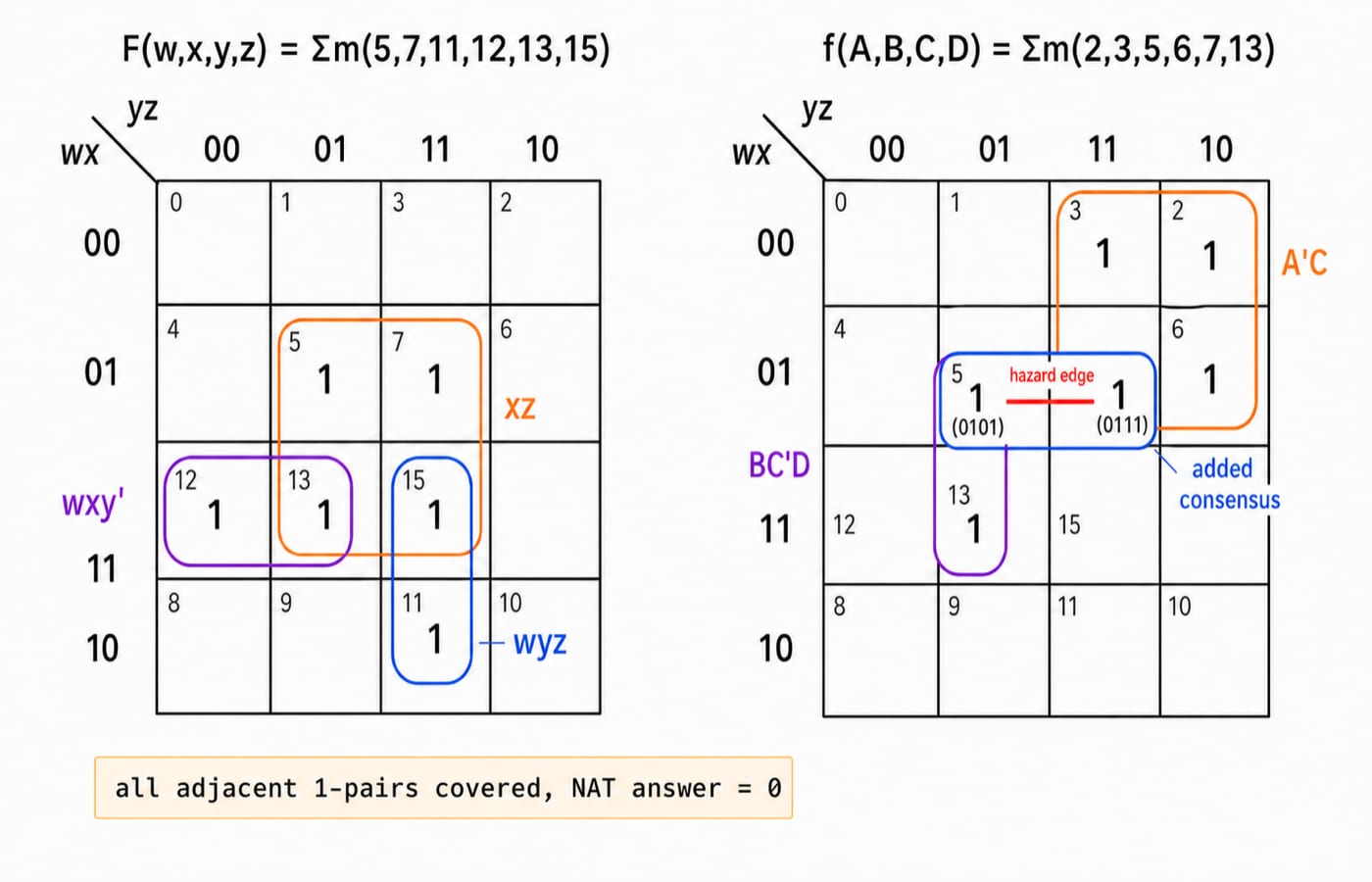
F(w,x,y,z) = Σm(5,7,11,12,13,15)
The function is implemented using a two-level minimal SOP realization (AND–OR circuit). It is known that such minimal SOP implementations are sometimes prone to static hazards.
Determine whether the circuit exhibits a static-1 hazard. If yes, specify the decimal minterm positions (input combinations) at which the hazard can occur. Give your answer as the sum of all such minterm indices.
Answer: ______
Answer: 0.
The minimal SOP is F = xz + wxy' + wyz. Pairs (5,7), (5,13), (7,15) and (13,15) share xz; (11,15) shares wyz; (12,13) shares wxy'. Every adjacent 1-pair remains covered, so there is no hazard minterm and the sum is 0.
Question 6: identify the one hazardous single-bit transition
The Boolean function is implemented using a two-level SOP (AND–OR) circuit:
f(A,B,C,D) = Σm(2,3,5,6,7,13)
This circuit may exhibit a static-1 hazard, i.e., a temporary glitch from logic ‘1’ to logic ‘0’ during certain input transitions.
Identify the input transitions for which the static-1 hazard can occur:
(a) Transition between minterms 2 (0010) and 3 (0011)
(b) Transition between minterms 5 (0101) and 7 (0111)
(c) Transition between minterms 6 (0110) and 7 (0111)
(d) Transition between minterms 7 (0111) and 13 (1101)
Answer: (b) Transition between minterms 5 (0101) and 7 (0111).
The cover is f = A'C + BC'D. Options (a) and (c) are safe because A'C covers both endpoints of the transition. In option (b) only C changes: BC'D covers minterm 5 and A'C covers minterm 7, with no product true throughout, so the output dips. Adding the consensus term A'BD covers both. Option (d) changes A and C together, so it is a possible function hazard, not the single-input logic hazard being asked for.
5. Glitch duration from unequal propagation paths
Question 7: subtract the two path delays
ISRO 2014
Consider the logic circuit given below.
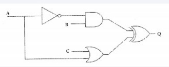
The inverter, AND and OR gates have delays of 6, 10 and 11 nanoseconds respectively. Assuming that wire delays are negligible, what is the duration of glitch for Q before it becomes stable?
(a) 5
(b) 11
(c) 16
(d) 17
Answer: (a) 5 ns. Practise the ISRO 2014 original
Input A reaches the XOR by two routes. The upper one runs through the inverter and the AND gate, 6 + 10 = 16 ns; the lower one runs through the OR gate, 11 ns. The XOR therefore sees mismatched inputs for 16 - 11 = 5 ns, and its own delay shifts that glitch without widening it. Neither 11 nor 16 is the answer.
Question 8: activate both terms and find the 7 ns gap
ISRO 2018
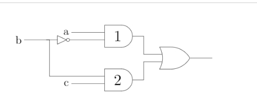
In the diagram above, the inverter (NOT gate) and the AND-gates labeled 1 and 2 have delays of 9, 10 and 12 nanoseconds(ns), respectively. Wire delays are negligible. For certain values of a and c, together with certain transition of b, a glitch (spurious output) is generated for a short time, after which the output assumes its correct value. The duration of the glitch is
(a) 7 ns
(b) 9 ns
(c) 11 ns
(d) 13 ns
Answer: (a) 7 ns. Practise the ISRO 2018 original
For ab' + bc, set a = c = 1 and let b fall. The output remains 1 as bc hands over to ab'. The terms switch at 12 ns and 19 ns (9 + 10), so the false 0 lasts 19 - 12 = 7 ns.
6. Timing waveforms, feedback and equal-delay pulses
Question 9: count four feedback-loop output changes
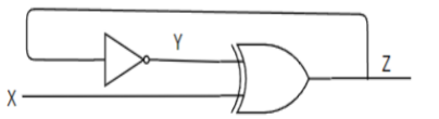
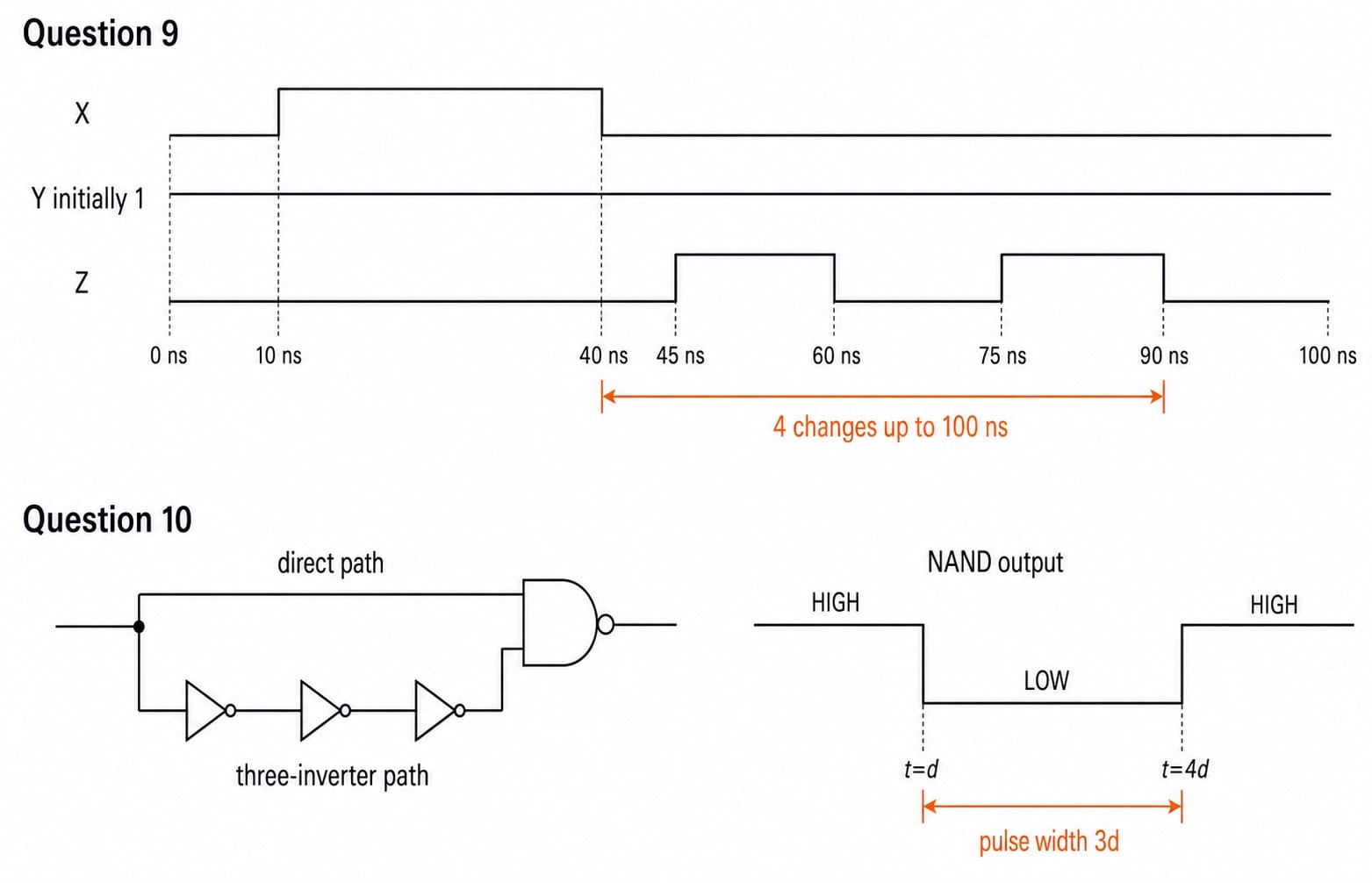
Assume that the inverter in the network below has a propagation delay of 10 ns and the XOR gate has a propagation delay of 5 ns. Draw the timing diagram for the network showing X, Y and Z. Take Y as initially 1; the waveform for X is given. The number of points where the level changes at output Z (excluding t = 0 ns, if any) up to t = 100 ns is _____.

Answer: 4.
Exclude any change at t = 0. The loop delay is 10 + 5 = 15 ns. With X = 1 from 10 ns to 40 ns, two inversions hold Z. After X returns to 0, the odd-inversion loop toggles Z at 45, 60, 75 and 90 ns. The next change is beyond 100 ns, so the count is 4.
Question 10: follow the direct and three-inverter paths
Consider the logic circuit with input signal shown in the figure. All gates in the figure shown have identical non-zero delay. The I/P signal which was at logic LOW is switched to logic HIGH and maintained at logic HIGH. The output
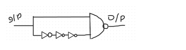
(a) pulses from LOW to HIGH to LOW
(b) stays LOW throughout
(c) stays HIGH throughout
(d) pulses from HIGH to LOW to HIGH
Answer: (d) pulses from HIGH to LOW to HIGH.
Let each gate delay be d. Initially the direct NAND input is 0, the three-inverter input is 1 and the output is HIGH. After I/P rises, the direct path makes the output fall at t = d. The lower branch reaches 0 at 3d, so the NAND output rises at 4d. It is LOW from d to 4d: HIGH -> LOW -> HIGH, with width 3d.
7. Hazards and timing questions: diagnose the miss and take the next step
If Questions 1 and 2 went wrong, the three hazard families are still blurring together. Questions 3, 5 and 6 expose consensus and adjacency gaps, and Question 4 tests fault counting rather than timing. For Questions 7 to 10, put every path arrival on one timeline before deciding anything.
Use this correction checklist:
Identify the intended stable output.
Find every reconvergent path.
Add gate delays along each path.
Mark the interval in which no product term or gate-input combination preserves the intended value.
For a static-1 SOP hazard, test every adjacent pair of 1-minterms and add the consensus implicant that spans the pair no single product covers. Combinational Circuits: MUX, Decoders, Adders puts these same gates in their wider setting.
Use GATE Guidance by Sanchit Sir to work this sequence in order, and GATE CS Exam Preparation for the courses and test series built around the paper. Then redo Questions 5, 7, 9 and 10 with the answers covered: they test K-map coverage, path subtraction, feedback timing and equal-delay tracing in turn.
Keep learning

Special Logic Circuits MCQs: 12 Solved Questions on Adders, Encoders, PLA and DAC
Solve 12 special logic circuits MCQs covering recognition, hardware counts, Boolean identities and numerical calculations. Each answer includes the reasoning you should reproduce in an exam.
19 Sep 20268 min readDigital Electronics MCQs

Function Equivalence MCQs: 12 Solved Boolean Algebra Problems
Solve 12 function-equivalence questions step by step, from De Morgan's law and absorption to minterm sets, counterexamples and a four-option MSQ.
Updated 17 Sep 20268 min readDigital Electronics MCQs

CLA & Arithmetic Logic MCQs: 10 Solved Questions with Explanations
Solve ten CLA and arithmetic logic MCQs with compact workings for carry equations, timing paths, hardware sizing and operand-pair counting.
Updated 16 Sep 20267 min readDigital Electronics MCQs

Sync Counter Design MCQs: 11 Solved Questions on Modulus, State Sequences and Excitation Logic
Solve 11 synchronous-counter questions covering modulus boundaries, repeated outputs, common-clock tracing, excitation equations, enables and composite states.
Updated 14 Sep 20267 min readDigital Electronics MCQs