Synchronous Counter Design: A MOD-6 JK Flip-Flop Worked Example
Build a MOD-6 synchronous up counter from its state sequence to its JK input equations, then verify valid states, recovery paths, and clock timing.
KnowledgeGate Team
Exam prep & CS education
Updated 29 Aug 20265 min read52 views

Drawing a count sequence is easy; turning it into correct flip-flop input equations becomes confusing when several bits change at one clock edge and unused states might lock the circuit. A three-bit synchronous MOD-6 up counter counts 000, 001, 010, 011, 100, 101, 000, recovers from 110 and 111, and meets a numerical clock-period constraint. Starting from already-given equations is synchronous counter analysis; design runs in the opposite direction, from a required sequence to six JK input functions. For the flip-flop foundation, review Sequential Circuits: Flip-Flops and a Worked Counter Design.
What makes a counter synchronous
A counter is a sequential circuit whose next state depends on its present state. In a synchronous counter, every flip-flop receives the same active clock edge, with input logic computed from the present outputs beforehand.
A ripple counter instead uses one stage's output to clock the next. Here, Q2 is the most significant bit, Q0 is the least significant bit, and Q2Q1Q0 names the state. Several outputs can respond to one edge, as in 011 -> 100, but settle only after clock-to-Q delays.
Keep three ideas separate: modulus is the number of states in the intended cycle, state encoding assigns bit patterns, and excitation logic tells each flip-flop what to do next.
Translate the MOD-6 specification into states
The required storage is
n = ceil(log2 6) = 3.
Three flip-flops provide 2^3 = 8 encodings. Six are used; 110 and 111 are unused. floor(log2 6) = 2 cannot work because two flip-flops represent only four states.
Fix the cycle before deriving gates:
0 -> 1 -> 2 -> 3 -> 4 -> 5 -> 0
000 -> 001 -> 010 -> 011 -> 100 -> 101 -> 000
This is a modulo-6 up counter, not a modulo-8 counter with two outputs hidden. Write the state table, apply the JK excitation table, minimise each input, draw the common-clock circuit, then verify intended and unused states.
Worked example, part 1: build the transition table
decimal | present | next | bits that change |
|---|---|---|---|
0 |
|
|
|
1 |
|
|
|
2 |
|
|
|
3 |
|
|
|
4 |
|
|
|
5 |
|
|
|
Read each row bit by bit. For 001 -> 010, Q2 holds at 0, Q1 changes 0 -> 1, and Q0 changes 1 -> 0. For 101 -> 000, Q2 and Q0 reset while Q1 stays at 0. This wrap makes ordinary binary-counter toggle rules fail.
Keep 110 and 111 outside the cycle for now. They can be don't-cares during minimisation, but substitute both into the final equations to test safety.
Worked example, part 2: derive the JK input equations
The JK excitation requirements are 0 -> 0: J=0,K=X; 0 -> 1: J=1,K=X; 1 -> 0: J=X,K=1; and 1 -> 1: J=X,K=0. Here, X is a don't-care.
transition |
|
|
|
|
|
|
|---|---|---|---|---|---|---|
| 0 | X | 0 | X | 1 | X |
| 0 | X | 1 | X | X | 1 |
| 0 | X | X | 0 | 1 | X |
| 1 | X | X | 1 | X | 1 |
| X | 0 | 0 | X | 1 | X |
| X | 1 | 0 | X | X | 1 |
For example, 001 -> 010 gives J2=0,K2=X; J1=1,K1=X; and J0=X,K0=1. For 011 -> 100, the entries are J2=1,K2=X; J1=X,K1=1; and J0=X,K0=1. The Flip-Flop Conversion for GATE refresher explains this transition-to-input method in more depth.
Minimisation gives:
J0=1,K0=1J1=not(Q2)Q0,K1=Q0J2=Q1Q0,K2=Q0
Thus Q0 always toggles. Q1 is set at 001 and reset when it is 1 with Q0=1. Q2 is set at 011 and reset at 101.
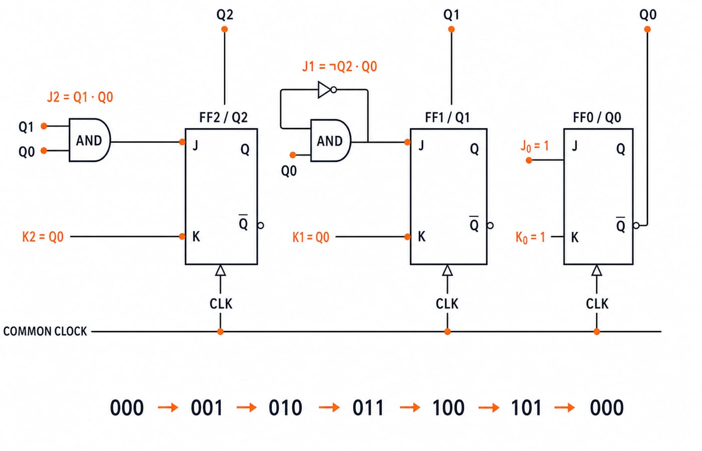
Worked example, part 3: verify the cycle and unused-state recovery
All inputs come from the same present state before the shared edge. At 001, J1=1 sets Q1 and K0=1 resets Q0, giving 010. At 011, J2=K2=1 toggles Q2 high, J1=K1=1 toggles Q1 low, and K0=1 resets Q0, giving 100. At 101, K2=1 resets Q2, J1=0 leaves Q1=0, and K0=1 resets Q0, giving 000.
Now test the unused states. At 110, Q0=0, so J1=K1=J2=K2=0, while J0=K0=1. Therefore 110 -> 111. At 111, J2=K2=1, J1=0,K1=1, and J0=K0=1; every current 1 changes to 0, so 111 -> 000. This particular circuit recovers from either unused state within at most two active clock edges. That result belongs to these equations, not to every possible minimisation.
For samples k=0..6, the state sequence is 000, 001, 010, 011, 100, 101, 000. The waveform rows are Q2 = 0,0,0,0,1,1,0; Q1 = 0,0,1,1,0,0,0; and Q0 = 0,1,0,1,0,1,0.
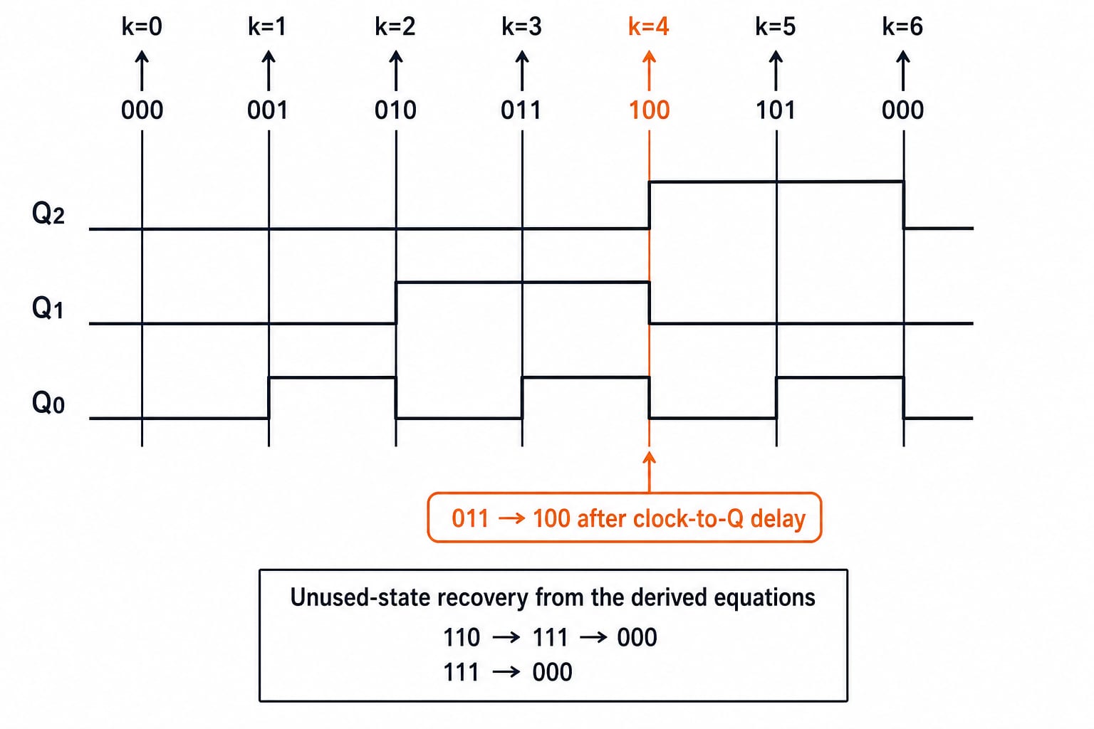
Timing limit: turn path delays into a clock frequency
With clock skew and uncertainty set to zero, the register-to-register timing condition is:
Tclk >= tCQ(max) + tlogic(max) + tsetup.
The path runs from a present-state Q, through input logic, to a receiving J or K before setup time. For hypothetical supplied values tCQ(max)=2 ns, tlogic(max)=5 ns, and tsetup=1 ns:
Tclk(min) = 2 ns + 5 ns + 1 ns = 8 ns
fmax = 1 / 8 ns = 125 MHz.
Do not add three flip-flop propagation delays merely because there are three stages. All stages share one clock, so the longest register-to-logic-to-register path controls this simplified calculation.
Design traps and common exam-style checks
trap | what goes wrong | correct check |
|---|---|---|
Use | Too few encodings | Use |
Forget | Builds the wrong wrap | Test the last row |
Clock one flip-flop from another | Creates a ripple counter | Trace one common clock |
Ignore unused states | Can hide lockout | Substitute every unused state |
Mix characteristic and excitation tables | Produces wrong inputs | Start from each required transition |
Claim zero-delay output changes | Ignores physical delay | Include clock-to-Q settling |
Practice can ask you to identify a modulus, find the flip-flop count, complete a state row, derive an input equation, test recovery, or calculate frequency from supplied delays. The supplied state sequence, equations, and delay values determine each result.
Use this 30-second check: count six unique states; test 011 -> 100 and 101 -> 000; substitute 110 and 111; then confirm Tclk(min)=8 ns and fmax=125 MHz under the stated assumptions. For a broader study route, continue with GATE CS Exam Preparation.
Synchronous counter design: the short version and next step
Retrieve the chain in order: M=6; ceil(log2 6)=3; cycle 000 through 101; JK excitation rows; six minimised inputs; valid-cycle substitution; unused-state recovery; and the register-to-register timing check. Now recreate the excitation rows for 001 -> 010, 011 -> 100, and 101 -> 000. Derive J1=not(Q2)Q0 and J2=Q1Q0, then prove 110 -> 111 -> 000 without looking back. Your timing self-check is 2 ns + 5 ns + 1 ns = 8 ns, hence 125 MHz. Use GATE Guidance by Sanchit Sir for a sequenced Digital Logic learning route. Once the state-table method is stable, move to timed practice.
Keep learning
NOT, OR and AND Gates: Evolution, Truth Tables and a Worked Circuit
Learn how NOT, OR and AND gates developed from switching ideas, then trace F=(A+B')C node by node and confirm it with a complete truth table.
Updated 23 Oct 20265 min readDigital Logic

Binary Arithmetic Operations Explained: Rules and Worked Examples
Learn binary addition, subtraction, multiplication and division with aligned worked examples, then separate carry, borrow and two's-complement overflow.
Updated 19 Oct 20266 min readDigital Logic

1's Complement Explained: Binary Conversion, Addition and Worked Examples
Learn how fixed-width 1's complement numbers represent negatives, why zero has two encodings, and how end-around carry works through exact examples.
Updated 15 Oct 20266 min readDigital Logic
Decimal Conversion Explained: Binary, Octal and Hexadecimal Worked Examples
Learn one dependable method for converting values between decimal, binary, octal and hexadecimal, including fractions, shortcuts and checks.
Updated 11 Oct 20265 min readDigital Logic