

Register & Bus Organization Explained: Worked Common-Bus Design and Exam Traps
Build a precise mental model of registers, a common bus and clocked transfer. Then trace R2 <- R5 through an exact 8-register, 16-bit datapath.
KnowledgeGate Team
Exam prep & CS education
Updated 6 Nov 20266 min read

R2 <- R5 looks simple, but questions mix up source, destination, bus width, selector count, multiplexer count, and values before and after a clock edge. A reliable trace separates combinational source selection from clocked destination loading. Use core CS fundamentals for the surrounding vocabulary, and CPU Organization Basics: Registers, Instruction Cycle and Worked Examples for the whole-processor path through PC, MAR, MDR, IR, and a complete LOAD-ADD-STORE cycle. By contrast, R2 <- R5 isolates the common bus: R5 drives one shared path, R2 receives the enabled load, and the edge changes stored state.
Registers, Buses and RTL: Build the Mental Model First
A register is a clocked group of flip-flops storing one binary word. Here each register is 16 bits, so R5 = 0x3A6C means 16 stored bits. Registers may hold operands or results; role-specific examples are the program counter (PC), instruction register (IR), memory address register (MAR), and memory data register (MDR). Real processors may organise them differently.
A bus is a shared set of parallel lines carrying one word. Keep three quantities separate: eight candidate source registers, a 16-bit bus, and three source-select bits. Eight registers do not make an 8-bit bus.
In register-transfer notation, P: R2 <- R5 means condition P enables the action, R5 is the source, and R2 the destination. R5 remains unchanged. The bus carries the value during the active interval, but R2 captures it only at the active clock edge. Comma-separated assignments are simultaneous only if the datapath provides the required paths.
How an 8-Register, 16-Bit Common Bus Is Built
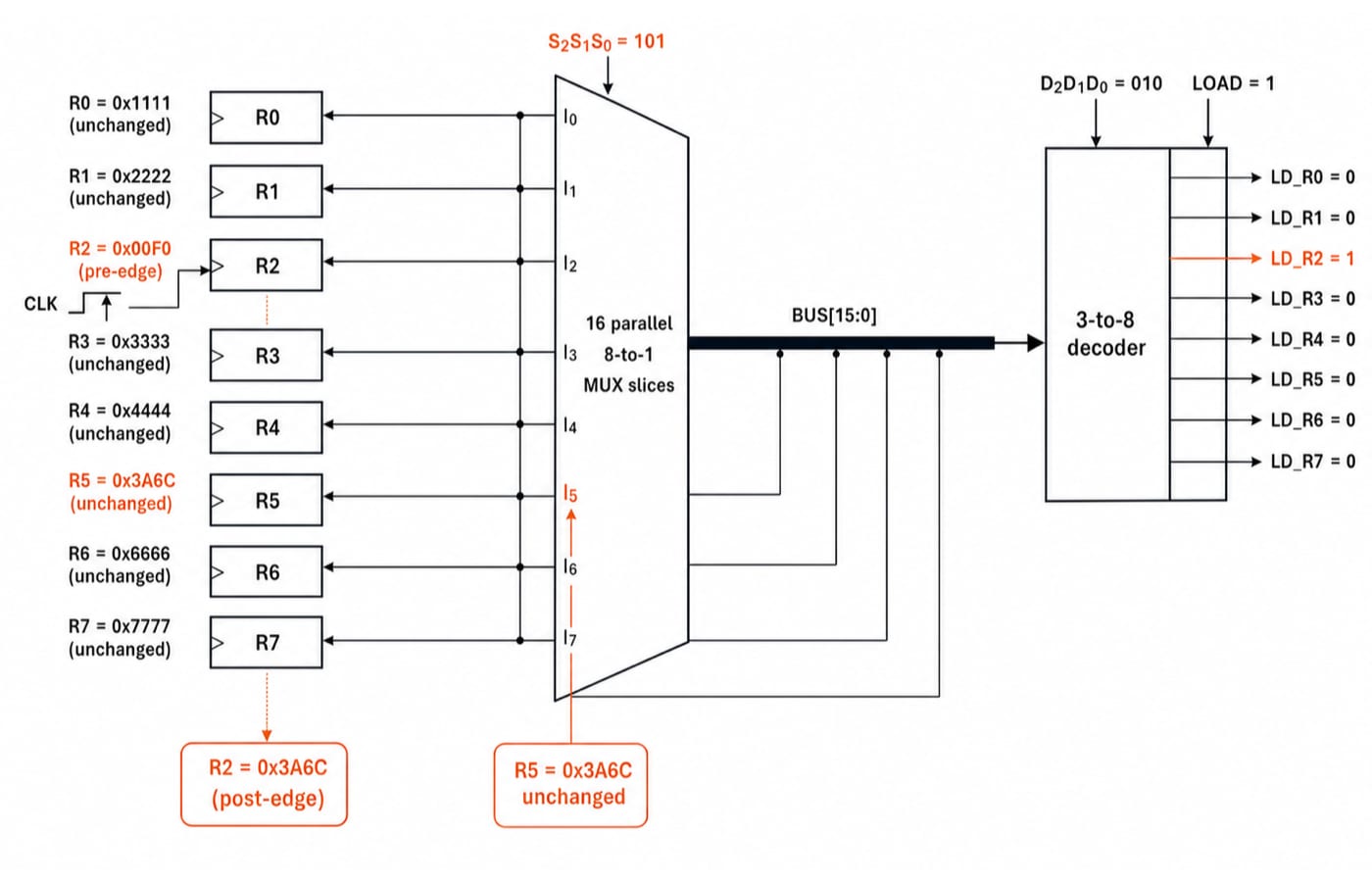
For eight registers R0 to R7, each 16 bits wide, the multiplexer construction uses 16 parallel 8-to-1 multiplexers. One multiplexer produces each bus bit. For example, the slice for BUS[6] receives bit 6 from all eight registers. All 16 slices share the source selector S2S1S0.
This is one 16-bit common bus, not 16 separate word buses. Each slice handles one bit position; shared controls keep all positions aligned during transfers.
The selector needs ceil(log2 8) = 3 bits. Assume the binary-index mapping 000 selects R0, 001 selects R1, and so on through 111 for R7. Therefore, 101 selects R5. If a question gives another mapping, use that mapping.
Destination control is separate. A 3-to-8 decoder receives D2D1D0, and a master LOAD signal enables loading. With the same binary-index convention, D2D1D0 = 010 and LOAD = 1 assert only LD_R2. Selecting R5 places its word on the bus. It does not, by itself, change R2 or any other register.
Fully Worked Transfer: Execute R2 <- R5 Without Skipping the Clock Edge
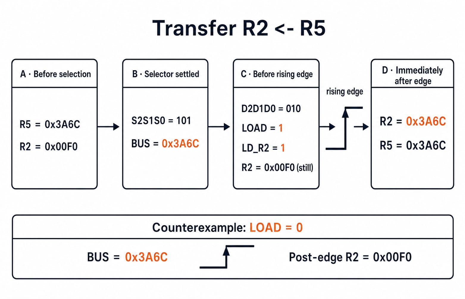
Start with R5 = 0x3A6C, R2 = 0x00F0, S2S1S0 = 101, D2D1D0 = 010, and LOAD = 1. All registers are positive-edge triggered. The bus value before the controls settle is irrelevant or unspecified, not automatically zero.
Trace the transfer through four checkpoints:
Source code
101selectsR5.The 16 multiplexer outputs produce
BUS[15:0] = 0x3A6C. In binary, that is0011 1010 0110 1100.The destination decoder asserts
LD_R2 = 1, so onlyR2is permitted to capture the bus. Before the edge,R2still contains0x00F0.At the rising edge,
R2changes from0x00F0to0x3A6C.R5and every other register retain their values.
The hardware answers follow directly. Multiplexer count equals bus width, so there are 16 multiplexers. Each has eight inputs because there are eight possible sources. Source-select width is log2 8 = 3 bits. Destination selection uses a 3-to-8 decoder. The transfer moves 16 data bits. Answers such as eight multiplexers, 16-to-1 multiplexers, or four selector bits confuse different dimensions.
Now change one control. If LOAD = 0, the bus can still show 0x3A6C, but R2 remains 0x00F0 after the edge. If D2D1D0 = 011 and LOAD = 1, R3, not R2, captures 0x3A6C.
Multiplexers, Tri-State Drivers and Bus Contention
Textbooks commonly show two implementations of the same source-selection idea. The multiplexer design selects one of eight inputs inside each of 16 bit slices. A tri-state design connects every register to the shared lines through enabled output drivers. At bit level, eight 16-bit registers require 8 x 16 = 128 tri-state output drivers.
A disabled tri-state output is high impedance, written Z. It does not drive the line, and it is neither a stored zero nor a stored one. Exactly one source bank may drive the bus at a time.
If R5 = 0x3A6C and R1 = 0x2222 drive the bus simultaneously, disagreeing bit positions face conflicting electrical drive. The result is not a valid bitwise OR, XOR, or predictable hexadecimal value.
What Bus Width Changes, and What It Does Not
A 16-bit bus carries at most 16 data bits per transfer interval. Moving the 32-bit value 0xABCD1234 between paired 16-bit register halves therefore needs at least two bus transfers, one for 0xABCD and one for 0x1234. Each transfer must enable the corresponding destination half.
Expanding from eight to 16 candidate 16-bit sources does not change the 16 bus lines or the count of 16 multiplexers. It changes every slice to 16-to-1 and increases the selector to log2 16 = 4 bits. A single common bus normally carries one selected source word at a time, so independent transfers may require separate cycles. A multibus datapath or a ported register file can move more than one word per cycle; the single-bus limit comes from the shared path.
Register and Bus Organization Traps to Correct Explicitly
Trap | Why it fails | Correct check |
|---|---|---|
Bus width equals register count | Confuses sources with lines | Count word bits |
Selector bits equal bus bits | Selector encodes sources | Use |
RTL direction reversed | Arrow marks destination | Read right to left |
Source cleared | Transfer copies | Source unchanged |
All registers load | Connection does not enable | Check load |
|
| Keep distinct |
Two sources enabled | Drivers contend | Enable one |
For n m-bit source registers, use m multiplexers of size n-to-1 and ceil(log2 n) selector bits. Ten 12-bit registers need 12 10-to-1 selections and four selector bits, since ceil(log2 10) = 4. Of 16 codes, six are unused or design-assigned.
Selection changes the bus combinationally. Stored state changes only with load at the active clock edge.
How Exam-Style Questions Test This Topic
Common COA practice asks you to interpret RTL, identify register roles, count multiplexers and selector bits, choose the register changed by a control word, distinguish bus width from source count, recognise high impedance, or trace values across a clock edge. Different exams combine these tasks differently, but each answer follows from the same datapath rules.
For this design, keep the exact anchors together: 16 multiplexers, each 8-to-1; three source-select bits; BUS = 0x3A6C before the edge; R2 = 0x3A6C only after the enabled rising edge; and R5 unchanged. With 16 sources and a 16-bit bus, the answer becomes 16 parallel 16-to-1 multiplexers and four selector bits.
After tracing the controls, use Computer Organization MCQs for broader COA practice.
The Short Version and the Next Practice Step
Count bus bits for the number of multiplexers. Count sources for multiplexer size. Take ceil(log2 n) for selector width. Then separate the value driven on the bus from the destination value captured at the clock edge.
Try this: for 16 registers of 32 bits, derive 32 16-to-1 multiplexers, four source-select bits, and a 4-to-16 destination decoder. Then trace R12 = 0x89ABCDEF into R3 using source code 1100 and destination code 0011.
For a broader computer science route, use ZERO TO HERO. For structured GATE preparation, use GATE Guidance by Sanchit Sir.
Keep learning
Register & Bus Organization MCQs: 12 Solved Questions with Explanations
Work through 12 Register and Bus Organization PYQs on CPU registers, micro-operations, common-bus multiplexers, tri-state drivers and register windows.
Updated 29 Oct 20267 min readComputer Organization MCQs

Register Transfer and Microoperations in COA: RTL Notation, Bus Design, and Every Microoperation Type with Worked Examples
RTL becomes easy when you treat every statement as parallel hardware action at one clock edge. This guide works through buses, subtraction, bit masks, insertion, and signed shifts.
Updated 2 Aug 20266 min read89 viewsComputer Organization & Architecture

Security, Risk Management and Maintenance in System Analysis and Design: A Worked Risk Register
Follow one university registration system from testable security requirements through risk ranking, maintenance classification, and a controlled production change.
Updated 7 Nov 20266 min readGATE Strategy & Roadmap

Direct Memory Access (DMA) Explained: Bus Cycles, Transfer Modes and a Worked Example
DMA becomes easier when you trace bus ownership, addresses and timing as one transfer. This guide follows a 6 KiB block through burst, cycle-stealing and transparent modes.
Updated 30 Oct 20266 min read137 viewsComputer Organization & Architecture