CPU Organization Basics: Registers, Instruction Cycle and Worked Examples
Follow PC, MAR, MDR, IR and AC through LOAD, ADD and STORE on a small 16-bit CPU. Then calculate opcode space, address capacity and common trace traps.
KnowledgeGate Team
Exam prep & CS education
Updated 31 Aug 20265 min read
A labelled CPU block diagram looks simple until a question asks what the PC, MAR, MDR, IR, accumulator and control unit contain after one instruction. Consider a 16-bit accumulator processor executing LOAD, ADD and STORE: its register values reveal exactly how control flow and data flow advance. Its deliberately small design isolates the instruction cycle; commercial processors add many details. For broader subject preparation, use GATE CS Exam Preparation.
CPU organization basics: what is being organized
CPU organization is the arrangement and interaction of the datapath, registers, ALU, control unit and buses while an instruction runs. Architecture usually means the programmer-visible contract, while organization describes its hardware implementation, although the boundary is not perfectly rigid.
For example, the meaning of LOAD belongs to the instruction-set architecture, while its temporary transfers through MAR and MDR belong to organization. Two implementations can expose the same instructions while using different internal data paths.
The processor uses von Neumann-style, word-addressable memory with a 16-bit accumulator. Memory and I/O sit outside the CPU. For every micro-operation, ask: what is the source, what is the destination, and which exact bits move?
Registers, ALU, control unit and buses in one datapath
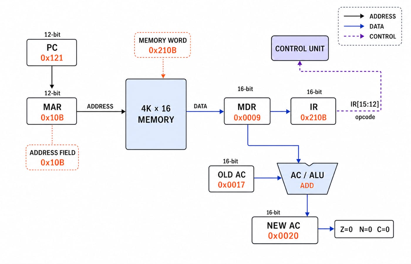
The 12-bit PC holds the next instruction address. The 12-bit MAR holds the address presented to memory, while the 16-bit MDR carries an instruction or data word. The 16-bit IR holds the current instruction. The 16-bit AC supplies an operand and receives the ALU result; status flags describe that result.
Common flags include zero (Z), negative (N) and carry (C). Their names are familiar, but their exact update rules remain part of the processor design.
The ALU performs the worked ADD. The control unit decodes IR and issues register-load, ALU-select, memory-read and memory-write signals. The processor has a 12-bit address path and a 16-bit data path, but not every CPU uses one shared physical bus.
Fetch, decode and execute as register-transfer steps
The fetch sequence is:
MAR <- PC
MDR <- M[MAR]
IR <- MDR
PC <- PC + 1
Ordering matters. After fetch, the incremented PC points to the next instruction while the current one still has to execute.
IR contains a 4-bit opcode in IR[15:12] and a 12-bit direct address in IR[11:0]. Here 0x1 means LOAD, 0x2 means ADD, and 0x3 means STORE; other patterns are reserved.
Execution follows these register transfers:
LOAD a:MAR <- a,MDR <- M[MAR],AC <- MDRADD a:MAR <- a,MDR <- M[MAR],AC <- AC + MDRSTORE a:MAR <- a,MDR <- AC,M[MAR] <- MDR
Worked CPU trace: LOAD 23, ADD 9, STORE 32
Use 16-bit words, 12-bit word addresses, initial PC = 0x120, and initial AC = 0x0000. Memory starts as follows:
Address | Initial word | Meaning |
|---|---|---|
|
|
|
|
|
|
|
|
|
|
| 23 decimal |
|
| 9 decimal |
|
| destination |
The PC changes during fetch, before execution.
Stage | PC | MAR | MDR | IR | AC | Memory change |
|---|---|---|---|---|---|---|
Fetch |
|
|
|
|
| none |
Execute |
|
|
|
|
| none |
Fetch |
|
|
|
|
| none |
Execute |
|
|
|
|
| none |
Fetch |
|
|
|
|
| none |
Execute |
|
|
|
|
|
|
The arithmetic is 0x0017 + 0x0009 = 0x0020, or 23 + 9 = 32. Under our unsigned 16-bit convention, the result is non-zero, its top bit is 0, and there is no carry beyond bit 15, so Z=0, N=0, and C=0.
The checkable final state is PC = 0x123, AC = 0x0020, and M[0x10C] = 0x0020. Source words M[0x10A] and M[0x10B] remain unchanged.
![Instruction-cycle timeline tracing LOAD, ADD and STORE through PC, IR, MDR and AC to final state PC 0x123, AC 0x0020, M[0x10C] 0x0020.](https://cdn.knowledgegate.ai/blog-assets/blog_asset_1784246002507_bbt4bu.jpg)
Bit widths and address capacity: a second worked calculation
A 4-bit opcode provides 2^4 = 16 opcode patterns. A 12-bit direct-address field selects 2^12 = 4096 word locations. With 16-bit words, total capacity is:
4096 x 16 = 65,536 bits = 8,192 bytes = 8 KiB
Therefore PC and MAR need 12 bits to name all 4096 words, while IR and MDR need 16 bits to hold one instruction or data word. The 8 KiB answer depends on word addressability. With the same 12 address bits in a byte-addressable system, the capacity would be 4096 bytes, or 4 KiB.
The instruction format supports only direct addressing. Addressing Modes and Instruction Formats explains how other formats interpret their operand fields. Real CPUs also use a memory hierarchy instead of waiting on main memory exactly as this trace does.
CPU organization traps that break otherwise correct traces
Mistake | Correction from this trace |
|---|---|
Treating PC as the current instruction after fetch | After fetching |
Swapping MAR and MDR | MAR holds address |
Changing IR during operand fetch | IR stays |
Adding hexadecimal as decimal text |
|
Assuming | AC remains |
Flags follow the convention supplied by the question. Here 0x0020 sets neither zero, negative nor carry, but designs can differ. Carry concerns a bit beyond the unsigned width; signed overflow concerns a signed result outside its range.
Write fetch and execute separately, pad values to their stated widths, and record memory changes only on writes. Always check the final state.
How exam-style questions test CPU organization basics
Common forms ask you to identify a register, order transfers, trace PC, IR and AC, calculate opcode or address capacity, or reject impossible data movement. Use this four-line self-test:
Before the third fetch,
PC = 0x122.After that fetch,
PC = 0x123andIR = 0x310C.After execution,
M[0x10C] = 0x0020.AC remains
0x0020.
Use the GATE Test Series for timed practice after you can reproduce the register trace. Then continue with Pipelining in Computer Architecture to study what changes when instruction execution overlaps.
CPU organization basics: the short version and next step
PC selects the next instruction; MAR and MDR connect the CPU to memory; IR and the control unit decode the current instruction; AC and the ALU produce the result. The final state PC = 0x123, AC = 0x0020, M[0x10C] = 0x0020 proves that you can follow control flow and data flow together. Redraw the datapath from memory, then reproduce the three-instruction trace without looking. For structured wider GATE CS study, continue with GATE Guidance by Sanchit Sir.
Keep learning

Pipelining Basics in Computer Architecture: Clock Cycle, Speedup and Hazard Worked Examples
Learn how to calculate a pipeline clock, fill and drain time, finite-batch speedup, latency, throughput, and the cost of a load-use stall.
Updated 23 Oct 20266 min readComputer Organization & Architecture

Data Manipulation Micro-Operations in COA: Arithmetic, Logic and Shift Operations Worked Step by Step
Learn a fixed-width method for tracing arithmetic, logic, and shift micro-operations. Every example tracks register values, result bits, carry, and overflow.
Updated 19 Oct 20265 min readComputer Organization & Architecture
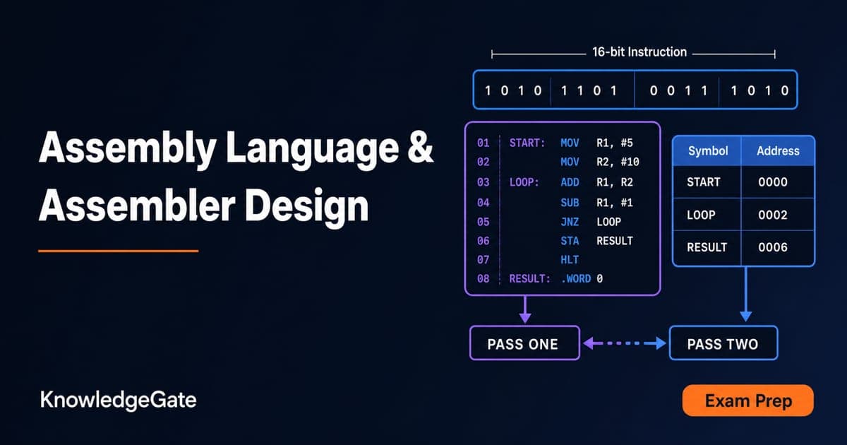
Assembly Language and Assembler Design: Two-Pass Translation with a Complete Worked Example
Follow a 16-bit Basic Computer program through pass one, pass two, hexadecimal encoding and execution, with every symbol, address and result shown.
Updated 15 Oct 20266 min readComputer Organization & Architecture

Computer Classification and Flynn’s Taxonomy: The Four Classes with a Worked Vector Example
A machine can belong to several computer classes at once. Learn the four classification axes, Flynn’s matrix, vector and multicore traces, and exam traps.
Updated 11 Oct 20266 min readComputer Organization & Architecture