In the diagram above, the inverter (NOT gate) and the AND-gates labeled 1 and…
2018
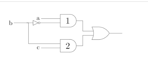
In the diagram above, the inverter (NOT gate) and the AND-gates labeled 1 and 2 have delays of 9, 10 and 12 nanoseconds(ns), respectively. Wire delays are negligible. For certain values of a and c, together with certain transition of b, a glitch (spurious output) is generated for a short time, after which the output assumes its correct value. The duration of the glitch is
Answer: A. 7 ns — The circuit implements the logic function Y = (a AND NOT b) OR (b AND c). A glitch (static-1 hazard) occurs when a=1 and c=1, as the output should remain 1…
- A.
7 ns
- B.
9 ns
- C.
11 ns
- D.
13 ns
Attempted by 215 students.
Show answer & explanation
Correct answer: A
The circuit implements the logic function Y = (a AND NOT b) OR (b AND c).
A glitch (static-1 hazard) occurs when a=1 and c=1, as the output should remain 1 while b transitions from 1 to 0.
The bottom path delay is 12 ns (AND gate). The top path delay is 9 ns (Inverter) + 10 ns (AND gate) = 19 ns.
The bottom path responds faster, dropping to 0 at t=12 ns. The top path takes longer to rise to 1, arriving at t=19 ns.
The output is 0 between t=12 ns and t=19 ns. Therefore, the glitch duration is 19 - 12 = 7 ns.
A video solution is available for this question — log in and enroll to watch it.