Sequential Circuits in Digital Electronics: Flip-Flops, Registers and a Worked Mod-4 Counter
Learn to trace sequential logic edge by edge, then design and verify a two-bit synchronous counter using state tables, D-input equations and timing constraints.
KnowledgeGate Team
Exam prep & CS education
Updated 13 Aug 20266 min read
A truth table feels manageable until a circuit feeds its old output back as part of its next input. Then state, clock edges and timing all matter. Flip-flops hold that state, registers group them into words, counters cycle them in a fixed order, and setup and hold times decide whether any of it survives at speed. Tracing a circuit edge by edge, rather than recalling device tables, is what sequential questions reward in GATE CS preparation, because one device table gives different answers depending on the active edge and the stored state.
What makes a circuit sequential?
A combinational block follows Y = f(X), so its present input determines its output. A sequential circuit stores state, and its next state follows Q(t+1) = f(Q(t), X(t)). The same present input can therefore lead to different results when the stored state differs. The combinational circuits guide works through multiplexers, decoders and adders, all on the memoryless side of that contrast.
In a synchronous design, memory elements hold Q. Combinational logic calculates the next state Q(t+1) and output Z. At an active clock edge, an edge-triggered flip-flop samples its input. A level-sensitive latch is instead transparent throughout its active level.
A Moore output depends only on state, Z = g(Q). A Mealy output may also depend on the present input, Z = g(Q,X). A Moore door alarm can depend on an ALARM state, while a Mealy warning can assert as soon as doorOpen=1 in the ARMED state.
Latches and flip-flops as state-transition rules
Read each device table as a rule for producing the next state.
Device | Inputs | Next-state rule |
|---|---|---|
Active-high NOR SR latch | S,R=00 / 10 / 01 / 11 | Hold / set / reset / forbidden |
D device | D=0 / 1 | Copy D at the active level or edge |
JK flip-flop | J,K=00 / 10 / 01 / 11 | Hold / set / reset / toggle |
T flip-flop | T=0 / 1 | Hold / toggle |
Asynchronous preset and clear, when provided, override normal clocked behaviour according to that device's data sheet.
For an exact JK trace, start at Q=0 and apply (J,K) = (1,0), (0,0), (1,1), (0,1) at four rising edges:
Edge 1 sets Q, so Q=1.
Edge 2 holds the state, so Q=1.
Edge 3 toggles 1 to 0, so Q=0.
Edge 4 resets Q, so Q=0.
The resulting trace is 1, 1, 0, 0. A characteristic table predicts the next state from the inputs. An excitation table works backwards from a required transition. For JK, the requirements are 0 to 0: J=0,K=X; 0 to 1: J=1,K=X; 1 to 0: J=X,K=1; 1 to 1: J=X,K=0, where X means don't-care. The flip-flops, latches and counters primer sets out the SR, D, JK and T characteristic tables in full and designs this same modulo-4 count with JK flip-flops.
Fully worked two-bit synchronous modulo-4 counter
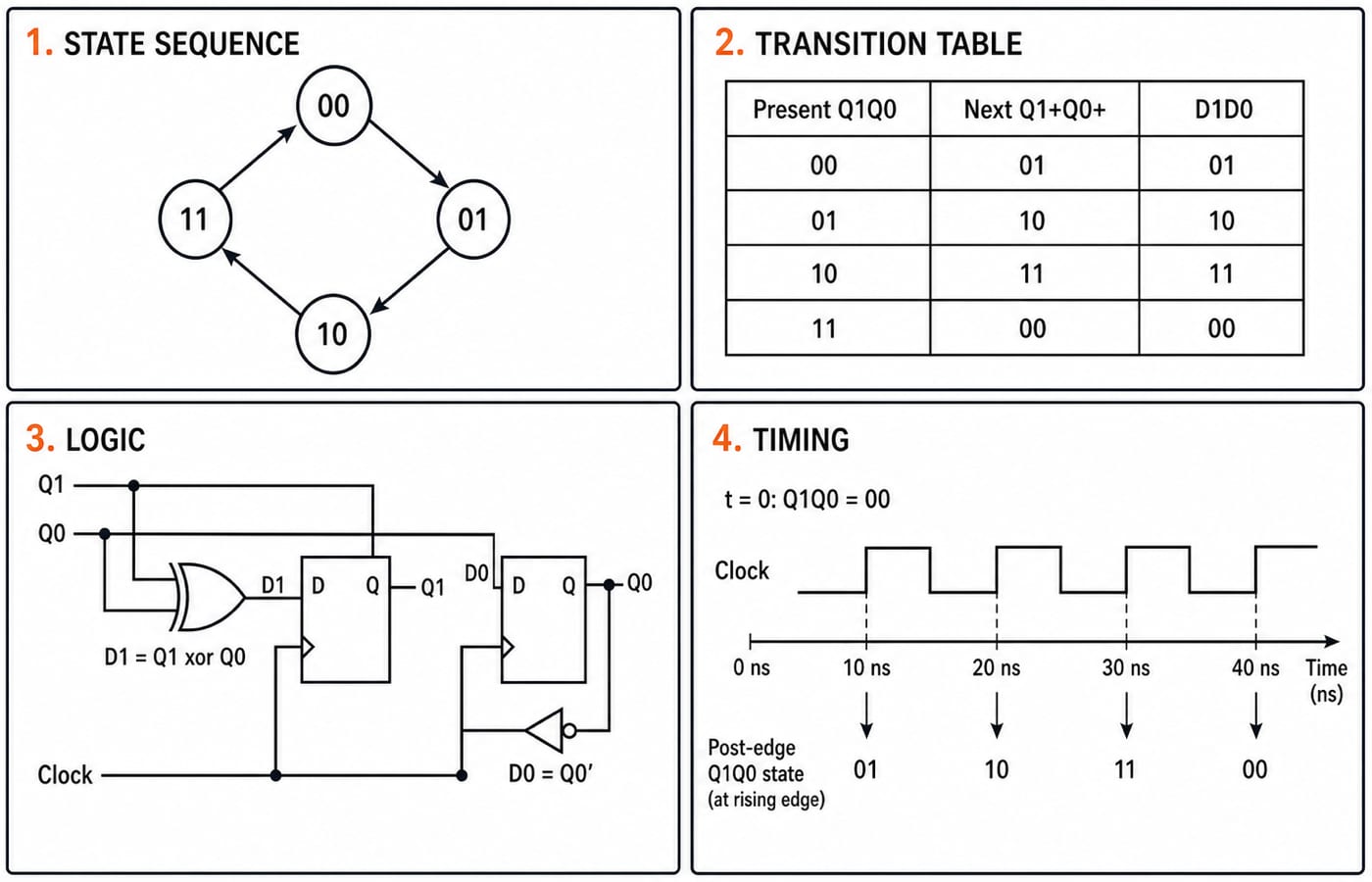
Design a counter with two rising-edge-triggered D flip-flops. Let Q1Q0 repeat 00 to 01 to 10 to 11 to 00, with Q1 as the most significant bit. Since a D flip-flop obeys D = Q(next), copy each next-state bit directly into D1 and D0.
Present Q1Q0 | Next Q1+Q0+ | D1D0 |
|---|---|---|
00 | 01 | 01 |
01 | 10 | 10 |
10 | 11 | 11 |
11 | 00 | 00 |
Across the rows, D0 is the complement of Q0, while D1 is 1 exactly when Q1 and Q0 differ. Therefore:
D0 = Q0'
D1 = Q1 xor Q0
Both flip-flops receive the same clock, so both state bits update together. The inverter and XOR form next-state logic, not extra memory.
Verify two rows numerically. At Q1Q0=10, D0=0'=1 and D1=1 xor 0=1, giving next state 11. At Q1Q0=11, D0=1'=0 and D1=1 xor 1=0, giving 00. Starting at 00 at t=0, rising edges at 10, 20, 30 and 40 ns produce post-edge states 01, 10, 11 and 00.
Registers and shift registers
An n-bit register uses n flip-flops sharing control signals. Parallel-in parallel-out (PIPO) loads and reads a whole word. Serial-in serial-out (SISO) takes and emits one bit per edge, serial-in parallel-out (SIPO) collects a serial stream into a parallel word, and parallel-in serial-out (PISO) sends a loaded word out bit by bit. A shift register moves its contents one position per active edge; a plain parallel register only loads or holds.
For a four-bit right shift, define Q3<-Sin, Q2<-Q3, Q1<-Q2, Q0<-Q1 at each rising edge. Start at Q3Q2Q1Q0=0000 and enter serial bits 1, 0, 1, 1:
Edge | Sin | Post-edge Q3Q2Q1Q0 |
|---|---|---|
1 | 1 | 1000 |
2 | 0 | 0100 |
3 | 1 | 1010 |
4 | 1 | 1101 |
The oldest bit reaches Q0 after four shifts. This behaviour supports serial-to-parallel conversion, temporary storage and delay lines.
Synchronous, ripple, ring and Johnson counters
In a synchronous counter, every flip-flop shares the clock. In a ripple counter, one stage's output clocks the next. Ideally, a three-bit binary counter driven at 1 MHz gives Q0=500 kHz, Q1=250 kHz and Q2=125 kHz, and has eight states from 000 through 111.
Ripple stages do not change simultaneously. Suppose a falling-edge-triggered three-bit counter has an 8 ns clock-to-Q delay per stage. For Q2Q1Q0: 011 to 100, the observable sequence is 011, 010 at 8 ns, 000 at 16 ns, then 100 at 24 ns. Logic decoding those temporary states can glitch. A rough delay-only frequency bound is 1/(3 x 8 ns) = 1/24 ns = 41.7 MHz, before device-specific margins.
A standard four-flip-flop ring counter circulates one asserted bit through four states. A standard four-flip-flop Johnson counter feeds back the complemented last output and can produce eight states. Different feedback or initialisation can change those results.
Setup, hold and the real timing limit
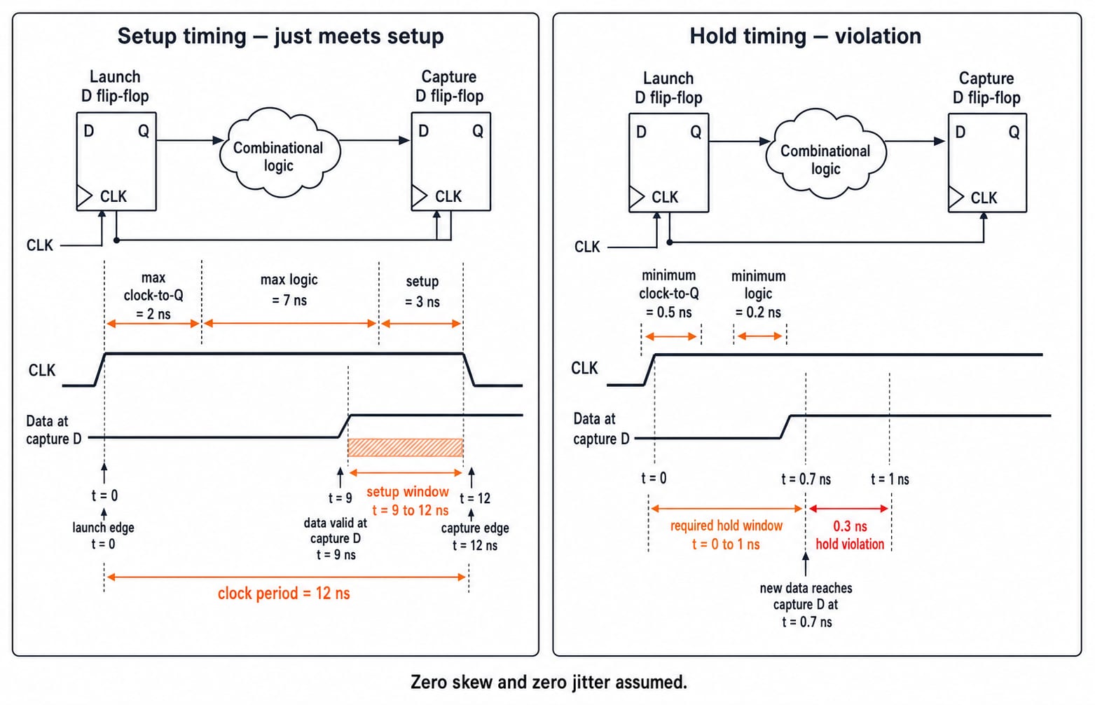
Setup time is how long D must be stable before the sampling edge. Hold time is how long it must remain stable after that edge. Clock-to-Q delay is the time from a launching edge until Q responds. A correct state table does not prove that a physical circuit meets timing.
Use hypothetical register-to-register values: maximum clock-to-Q is 2 ns, maximum logic delay is 7 ns, capture setup is 3 ns, and skew and jitter are zero. Then Tclock >= 2+7+3 = 12 ns, so the theoretical maximum frequency is 1/12 ns = 83.3 MHz. For a capture edge at t=12 ns, the setup deadline is t=9 ns. Data launched at t=0 reaches capture D at 2+7=9 ns, just meeting setup.
Check the minimum path separately. With minimum clock-to-Q of 0.5 ns and minimum logic delay of 0.2 ns, new data reaches D at 0.7 ns. A 1 ns hold requirement is therefore missed by 1-0.7=0.3 ns at zero skew. Any fix must be engineered for the actual path and device.
Common traps in exam-style questions
Correct the method before calculating:
Do not confuse a latch with a flip-flop. Mark the active level or edge first.
Do not inspect only a ripple counter's final state. Trace every intermediate transition.
Declare whether Q1 or Q0 is the most significant bit before building a table.
In an excitation table, X means don't-care, not a logic input value.
Identify synchronous or ripple construction before applying a frequency formula.
Typical questions ask you to find a next state, choose excitation inputs, derive D equations, trace a shifted word, calculate a modulus or divided frequency, or check setup and hold from supplied delays. Show the intermediate states or the timing inequality. KnowledgeGate carries over 100 sequential-circuits practice questions, covering latches, flip-flop conversion, shift registers, synchronous counter design and analysis, ripple counters and Johnson counters. The GATE Test Series puts them under exam timing.
Sequential circuits in one minute and what to do next
Identify the stored state, mark the active clock condition, write present and next states, select the storage element, derive its input equations, simulate every edge, then test setup, hold and propagation paths. The numbers to check yourself against are the JK trace 1, 1, 0, 0, modulo-4 cycle 00, 01, 10, 11, shift states 1000, 0100, 1010, 1101, and ripple settling at 24 ns.
Now rebuild the modulo-4 table and equations without looking. Then change the desired cycle to 00 to 10 to 11 to 01 to 00 and derive new D inputs. Number systems, Boolean minimisation, logic gates, combinational blocks and sequential circuits run in that order inside GATE Guidance by Sanchit Sir.
Keep learning

Functional Completeness in Digital Logic: NAND, NOR and Worked Examples
Learn what makes a Boolean operator set complete, how NAND and NOR recover a standard basis, and how to verify a four-gate NAND construction.
Updated 2 Oct 20266 min readDigital Logic
Boolean Function Counts: Formulas, Worked Examples and Exam Traps
Build the master Boolean-function formula from output choices, then learn how common restrictions change the count through combinations, pairing and inclusion-exclusion.
Updated 27 Sep 20266 min readDigital Logic

Analog-Digital Conversion Basics: ADC, DAC, Worked Examples and Exam Patterns
Build ADC and DAC basics from one consistent transfer model, then practise code selection, reconstruction error, flash and SAR conversion, and bit-depth calculations.
Updated 25 Sep 20266 min readDigital Logic

Universal Realization with NAND and NOR Gates: Concepts, Worked Example and Exam Patterns
Learn why NAND and NOR are universal, then implement one three-variable function using four NAND gates and four NOR gates with verified input traces.
Updated 23 Sep 20265 min readDigital Logic