Universal Realization with NAND and NOR Gates: Concepts, Worked Example and Exam Patterns
Learn why NAND and NOR are universal, then implement one three-variable function using four NAND gates and four NOR gates with verified input traces.
KnowledgeGate Team
Exam prep & CS education
Updated 23 Sep 20265 min read

Knowing that NAND and NOR are called universal gates is easy. The difficulty starts when a Boolean expression must become a circuit that uses only one gate type. NOT, AND and OR constructions establish completeness, and one three-variable function is realized with four NAND gates and four NOR gates. Use a repeatable SOP-to-NAND and POS-to-NOR method instead of memorising a circuit without reasoning.
Related reading: universal realization MCQs and NAND and NOR realization.
Universal realization: what “universal” actually means
A gate is universal if repeated copies of that one gate can construct NOT, AND and OR. These three operations can express any Boolean function, so a gate that can build all three is functionally complete. NAND alone is universal, and NOR alone is universal.
This is stronger than simply being a commonly used gate. AND, OR, XOR and XNOR are not individually universal under the standard gate-only interpretation. A NAND-only circuit may contain repeated NAND gates and tied inputs, but it cannot quietly use a separate inverter.
Use X' for complement, XY or X·Y for AND, and X+Y for OR. NAND is (XY)' and NOR is (X+Y)'; the output complement is part of each gate's definition.
NAND and NOR identities that prove functional completeness
For NAND, tie both inputs together to make an inverter:
NOT:
X'=X NAND XAND:
XY=(X NAND Y) NAND (X NAND Y)OR:
X+Y=(X NAND X) NAND (Y NAND Y)
The AND construction negates (XY)' once more. For OR, De Morgan's law gives X+Y=(X'Y')', exactly what the final NAND produces.
The NOR identities are the dual set:
NOT:
X'=X NOR XOR:
X+Y=(X NOR Y) NOR (X NOR Y)AND:
XY=(X NOR X) NOR (Y NOR Y)
Here the last identity follows from XY=(X'+Y')'. These are dual recipes, not unrelated tricks. The practical rule is equally neat: a simplified SOP expression naturally feeds a NAND-NAND structure, while a simplified POS expression feeds a NOR-NOR structure. Review De Morgan's law, SOP and POS in the Boolean Algebra and K-map Minimization Guide if that conversion feels abrupt.
Universal realization worked function: simplify before replacing gates
Use the same function for both circuits:
F(A,B,C)=A'B+BC
Factoring B gives F=B(A'+C). The first form is suitable for NAND gates, while the second is suitable for NOR gates. They are algebraically identical.
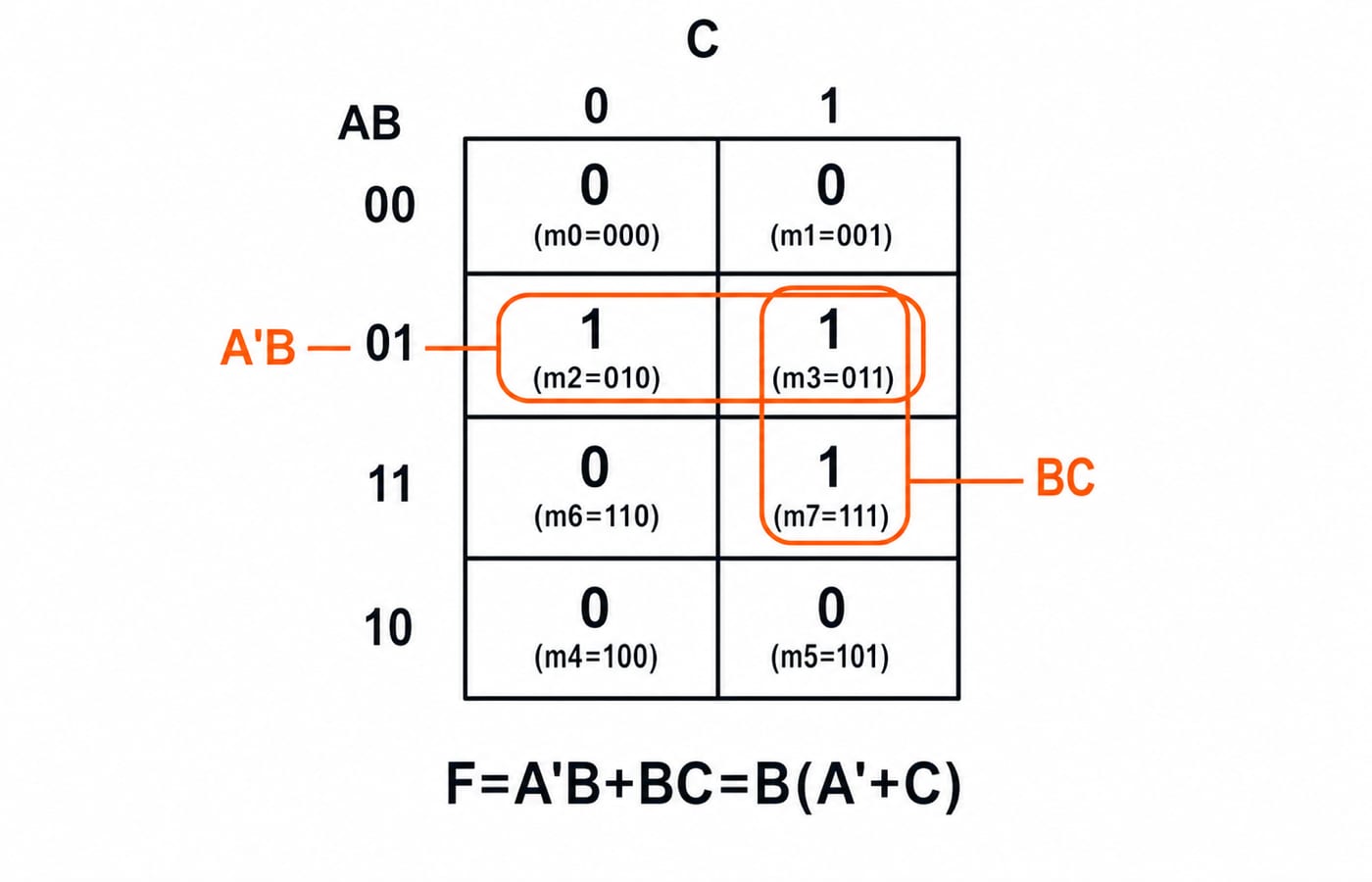
For variable order A,B,C, the function is F=Σm(2,3,7):
A | B | C | A'B | BC | F |
|---|---|---|---|---|---|
0 | 0 | 0 | 0 | 0 | 0 |
0 | 0 | 1 | 0 | 0 | 0 |
0 | 1 | 0 | 1 | 0 | 1 |
0 | 1 | 1 | 1 | 1 | 1 |
1 | 0 | 0 | 0 | 0 | 0 |
1 | 0 | 1 | 0 | 0 | 0 |
1 | 1 | 0 | 0 | 0 | 0 |
1 | 1 | 1 | 0 | 1 | 1 |
On a three-variable K-map, grouping m2,m3 produces A'B. Grouping m3,m7 produces BC. The overlap at m3 is valid because a 1 may help form more than one group. Therefore, the output vector is 0,0,1,1,0,0,0,1.
NAND-only realization: four gates, traced step by step
Apply De Morgan to the whole SOP expression:
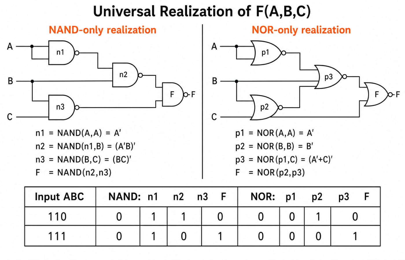
F=A'B+BC=((A'B)'(BC)')'
Now define four two-input NAND gates:
n1=NAND(A,A)=A'n2=NAND(n1,B)=(A'B)'n3=NAND(B,C)=(BC)'F=NAND(n2,n3)
For input 110, n1=0, n2=NAND(0,1)=1, and n3=NAND(1,0)=1. Hence F=NAND(1,1)=0. For 111, the nodes are n1=0, n2=1, n3=0, so F=1. Both results match the truth table.
The design has four physical NAND gates. The A path has three logic levels because producing A' adds a level. “NAND-NAND” names the two main realization stages after any required literal inversion, not two delays from every input.
NOR-only realization: the same function with the dual method
Start from F=B(A'+C) and rewrite it as F=(B'+(A'+C)')'. Use four two-input NOR gates:
p1=NOR(A,A)=A'p2=NOR(B,B)=B'p3=NOR(p1,C)=(A'+C)'F=NOR(p2,p3)
For 110, p1=0, p2=0, and p3=NOR(0,0)=1, so F=NOR(0,1)=0. For 111, p1=0, p2=0, and p3=NOR(0,1)=0, so F=1. The NOR circuit again matches the table.
Both designs use four gates and produce 0,0,1,1,0,0,0,1. The NAND route starts from SOP; the NOR route starts from POS.
Universal-gate conversion traps and quick correctness checks
The first trap is replacing gate symbols before choosing SOP or POS. Simplify first, choose NAND for SOP or NOR for POS, then apply De Morgan to the entire outer operation. A second trap is forgetting a tied-input inverter or cancelling only one of a pair of bubbles.
Another common error is calling a circuit NAND-only while using a separate NOT gate. Count every physical gate, including the NAND that creates A'. That is why the worked NAND circuit has four gates, not three. Also, XOR or XNOR does not become universal merely because a special constant input can produce a complement.
Before accepting a circuit, use three checks:
Expand every NAND or NOR node back into Boolean algebra.
Test one 0-output row such as
110and one 1-output row such as111.Compare the complete output vector when a minimum-gate or equivalence claim is involved.
Universal realization exam patterns: what to practise
Questions usually take one of four shapes: identify a universal gate, synthesize NOT, AND or OR from one gate type, convert an SOP or POS into a homogeneous circuit, or find the output or minimum gate count of a drawn network. Active-low bubbles and circuit-equivalence questions test the same De Morgan reasoning.
Use this decision rule under time pressure: simplify, select SOP for NAND or POS for NOR, label intermediate complements, and test a discriminating input. The 110 and 111 traces above are a model for evaluating an unfamiliar network. For further practice, solve Universal Realization questions that ask for output vectors, missing complements and gate counts.
Place this topic within the wider syllabus through GATE CS Exam Preparation. Then use the GATE Test Series for timed Boolean-algebra and circuit practice.
Universal realization: the short version and next step
NAND and NOR are each universal because they can build NOT, AND and OR.
Tie a gate's inputs together to make an inverter.
Map simplified SOP to NAND-NAND.
Map simplified POS to NOR-NOR.
Verify the algebra and at least two truth-table rows.
Universal realization is one way to implement a combinational Boolean function. The earlier Universal Gates for GATE: Realizing Any Function with Only NAND or Only NOR, and Counting the Minimum Gates focuses on bubble-pushing shortcuts, fan-in assumptions and XOR/XNOR minimum counts. Holding F=A'B+BC and its truth table constant exposes the exact duality between the four-gate NAND and NOR realizations.
Use GATE Guidance by Sanchit Sir if you want Digital Logic sequenced with the wider GATE CS syllabus. If this is your only weak point, first redraw both four-gate circuits from memory and verify all eight rows.
Keep learning

Functional Completeness in Digital Logic: NAND, NOR and Worked Examples
Learn what makes a Boolean operator set complete, how NAND and NOR recover a standard basis, and how to verify a four-gate NAND construction.
Updated 2 Oct 20266 min readDigital Logic

Boolean Function Counts: Formulas, Worked Examples and Exam Traps
Build the master Boolean-function formula from output choices, then learn how common restrictions change the count through combinations, pairing and inclusion-exclusion.
Updated 27 Sep 20266 min readDigital Logic

Analog-Digital Conversion Basics: ADC, DAC, Worked Examples and Exam Patterns
Build ADC and DAC basics from one consistent transfer model, then practise code selection, reconstruction error, flash and SAR conversion, and bit-depth calculations.
Updated 25 Sep 20266 min readDigital Logic

Special Logic Circuits: ROM, Majority Logic and Array Multiplier Examples
Learn one method for analysing special logic circuits, then apply it to majority logic, a BCD detector, programmable logic and two versions of a 4-bit multiplier.
Updated 22 Sep 20266 min readDigital Logic