Analog-Digital Conversion Basics: ADC, DAC, Worked Examples and Exam Patterns
Build ADC and DAC basics from one consistent transfer model, then practise code selection, reconstruction error, flash and SAR conversion, and bit-depth calculations.
KnowledgeGate Team
Exam prep & CS education
Updated 25 Sep 20266 min read
Remembering 2^n is not enough. Many learners still lose the calculation because they mix up the number of codes, the largest code, step size, and the treatment of the full-scale endpoint. Sampling selects signal values at discrete instants, quantisation assigns them to amplitude bins, binary encoding writes the bin index as an n-bit word, and a DAC maps the digital code to an analog output. The arithmetic is simple once the transfer convention is fixed, and that convention matters just as much as the formula. Use CS Fundamentals for Exams & Placements for the wider subject route.
What an ADC changes at each stage
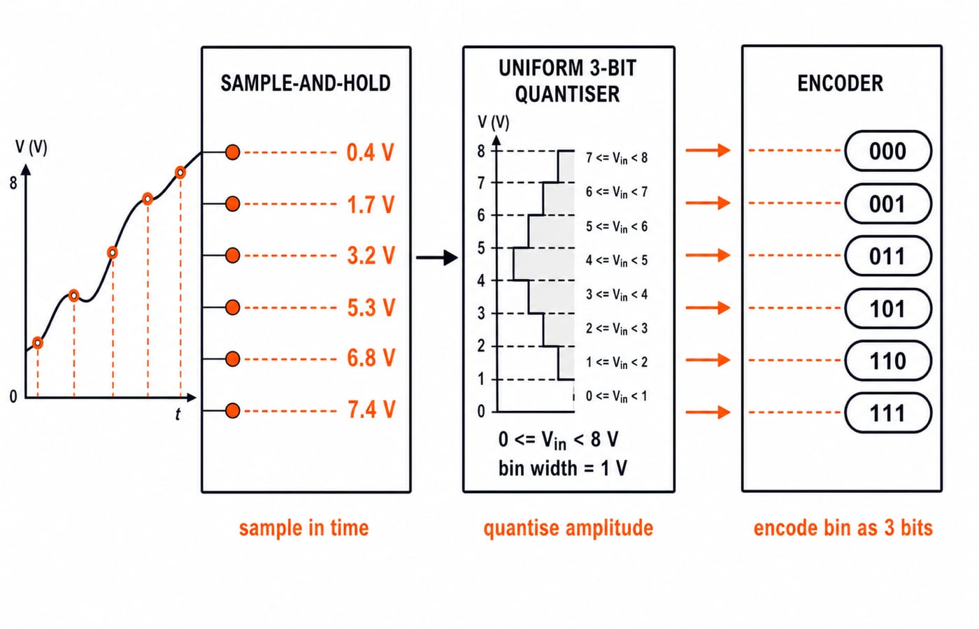
An analog input is continuous in both time and amplitude. Sampling selects its values at discrete instants, and a sample-and-hold circuit keeps each selected voltage stable during conversion. Quantisation then assigns the held value to one of a finite number of amplitude bins. Encoding writes that bin index as an n-bit word. A sampled signal is therefore not yet digital until its amplitude has also been quantised and encoded.
Use a 3-bit ADC with 0 <= Vin < 8 V, eight uniform 1 V bins, natural binary, and a lower-edge decision rule. Six held samples, 0.4, 1.7, 3.2, 5.3, 6.8, 7.4 V, enter decimal bins 0, 1, 3, 5, 6, 7. Their codes are 000, 001, 011, 101, 110, 111. The value 8 V is the upper range boundary, not a ninth bin. Any over-range or saturation behaviour must be stated by the problem or converter specification.
Codes, levels, step size, resolution and quantisation error
For an n-bit uniform unipolar ADC under this range-bin convention, keep these quantities separate:
Number of codes:
L = 2^nLargest unsigned code index:
L - 1 = 2^n - 1Volts per LSB, or step size:
Delta = (Vmax - Vmin)/2^n
For an in-range input, find k = floor((Vin - Vmin)/Delta) and encode decimal k in binary. Clamp k to 0 through 2^n - 1 only when the model explicitly specifies saturation. With midpoint reconstruction, Vhat = Vmin + (k + 0.5)Delta, and signed error is e = Vhat - Vin. For an ideal, uniform, unsaturated quantiser, its magnitude stays within half a step. Keep step size in volts per code.
Smaller steps improve ideal resolution, but resolution is not accuracy. Offset, gain error, noise, and non-linearity can still make a measured conversion inaccurate. If decimal-to-binary conversion causes trouble, revise Number Systems and Base Conversions Explained, especially fixed-width binary.
Fully worked 3-bit ADC conversion for 5.3 V
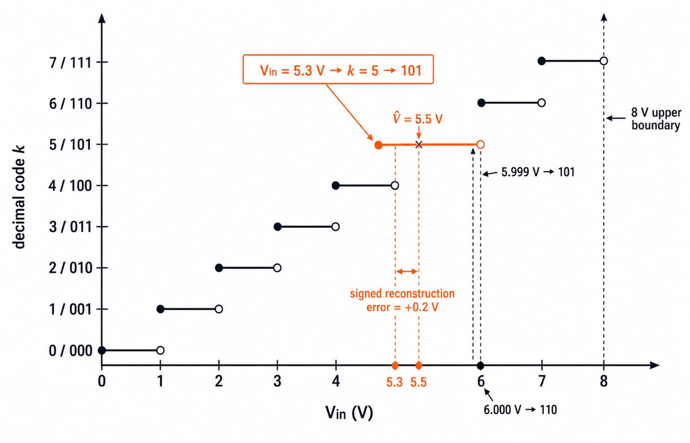
First state the complete model: an ideal uniform ADC with Vmin = 0 V, Vmax = 8 V, n = 3, natural binary, lower-edge quantisation, midpoint reconstruction, and in-range input Vin = 5.3 V.
Now calculate each line:
Number of codes:
L = 2^3 = 8.Step size:
Delta = (8 - 0)/8 = 1 V.Bin index:
k = floor((5.3 - 0)/1) = floor(5.3) = 5.Decimal
5written in three bits is101.The decision interval for code
101is[5, 6) V.Its midpoint reconstruction value is
Vhat = 0 + (5 + 0.5)(1) = 5.5 V.Signed reconstruction error is
e = 5.5 - 5.3 = +0.2 V.The error magnitude is
0.2 V, which is belowDelta/2 = 0.5 V.
Boundary checks must use the same lower-edge rule. At 5.999 V, floor(5.999) = 5, so the output remains 101. At 6.000 V, floor(6.000) = 6, so the output becomes 110. The floor operation is not casual rounding. It follows from the stated transfer model. Also, Vin = 8 V is outside the declared half-open range. A stated saturating model may map it to 111, but that behaviour cannot be assumed.
Reverse the direction with an ideal DAC
A DAC accepts a digital code and produces one of a finite set of analog output levels. It cannot recreate every original analog value. An ADC followed by a DAC normally gives a stepped approximation unless filtering and the time-domain model are also considered.
Take a 4-bit ideal unipolar DAC with Vref = 8 V and the stated rule Vout = (D/2^4)Vref. Input 1010_2 is decimal 10, so Vout = (10/16) x 8 = 5.0 V. One LSB is 8/16 = 0.5 V. The largest input, 1111_2 = 15, produces (15/16) x 8 = 7.5 V, not 8 V, under this rule. An endpoint-calibrated question may instead give a formula using 2^n - 1. Always follow the equation given in the question without mixing conventions.
Flash and SAR ADCs using the same 5.3 V input
Architecture changes the route to the code, not the final ideal code. A 3-bit flash ADC needs 2^3 - 1 = 7 comparators, with thresholds at 1, 2, 3, 4, 5, 6, 7 V. At 5.3 V, the first five thresholds have been crossed, so the priority encoder returns decimal 5, or 101.
A 3-bit successive-approximation conversion reaches the same result through three trials:
Try
100, corresponding to4 V. Since5.3 Vis higher, keep the most significant bit.Try
110, corresponding to6 V. Since5.3 Vis lower, clear the middle bit.Try
101, corresponding to5 V. Since5.3 Vis higher, keep the least significant bit.
The result after three compare-and-update decisions is 101. Flash makes threshold decisions in parallel, while SAR resolves one bit at a time. Encoders and related blocks are covered in Combinational Circuits: MUX, Decoders, Adders.
How exam-style problems test ADC and DAC basics
Exam-style problems typically ask for code count and step size, an input-voltage code, DAC output, required bit depth, flash comparator count, or a staircase boundary.
For a reverse bit-depth drill, suppose an ADC spans 0 to 5 V and requires Delta <= 10 mV = 0.01 V.
Required levels are at least
5/0.01 = 500.Therefore
n = ceil(log2 500) = 9.Eight bits provide only
2^8 = 256levels.Nine bits provide
2^9 = 512levels.The actual 9-bit step is
5/512 = 0.009765625 V, or about9.77 mV, so it meets the requirement.
Practise the calculation sequence under time pressure in the GATE Test Series: write the range, bit depth, and decision rule before calculating the code or voltage. Then explain why the chosen transfer convention controls the endpoint.
Traps that change an otherwise correct answer
Check these traps before finalising:
Trap | Consequence | Correction |
|---|---|---|
Swap | Wrong step and endpoint | Separate code count from largest code |
Mix the two step formulas | Inconsistent model | Write the transfer function first |
Ignore floor, rounding, or saturation | Wrong boundary code | State the decision rule |
Reuse a unipolar range for bipolar input | Wrong bin locations | Check the declared interval |
Treat bit depth as accuracy | Real errors are hidden | Separate resolution from offset, gain error, and noise |
Call sampling quantisation | Time and amplitude are confused | Sampling discretises time; quantisation discretises amplitude |
Finish by keeping units in volts, producing exactly n bits, checking the code from 0 to 2^n - 1, and comparing neighbouring staircase bins.
The short version and next study step
For an ADC, extract Vmin, Vmax, n, and the transfer convention. Calculate 2^n, calculate Delta, locate the input bin, encode its index, and check the boundary. For a DAC, convert the binary word to decimal and apply the transfer equation given in the question. If you need the wider GATE CS learning sequence, continue with GATE Guidance by Sanchit Sir. Then redo the 5.3 V example under a different stated convention and explain exactly why the answer changes.
Keep learning

Functional Completeness in Digital Logic: NAND, NOR and Worked Examples
Learn what makes a Boolean operator set complete, how NAND and NOR recover a standard basis, and how to verify a four-gate NAND construction.
Updated 2 Oct 20266 min readDigital Logic
Boolean Function Counts: Formulas, Worked Examples and Exam Traps
Build the master Boolean-function formula from output choices, then learn how common restrictions change the count through combinations, pairing and inclusion-exclusion.
Updated 27 Sep 20266 min readDigital Logic

Universal Realization with NAND and NOR Gates: Concepts, Worked Example and Exam Patterns
Learn why NAND and NOR are universal, then implement one three-variable function using four NAND gates and four NOR gates with verified input traces.
Updated 23 Sep 20265 min readDigital Logic
Special Logic Circuits: ROM, Majority Logic and Array Multiplier Examples
Learn one method for analysing special logic circuits, then apply it to majority logic, a BCD detector, programmable logic and two versions of a 4-bit multiplier.
Updated 22 Sep 20266 min readDigital Logic