Logic Gates in Digital Electronics: Truth Tables, Boolean Expressions and Worked Examples
Learn the seven basic logic gates, build and minimise a complete three-input truth table, then implement the result using only NAND gates. Hardware bubbles and delay paths are included.
KnowledgeGate Team
Exam prep & CS education
Updated 9 Aug 20265 min read
A logic gate question becomes confusing when the same operation appears as a symbol, a Boolean expression, a truth-table column, or one stage inside a larger circuit. The cure is to translate each form into small, checkable steps. Seven gate functions cover everything at this level, a three-input function has exactly eight rows to fill, and once those rows exist the minimisation and the NAND-only rebuild are mechanical. Calculating an output beats recognising a symbol, because the calculation still works when the symbol is unfamiliar.
Logic Gates: From Binary Inputs to One Output
A logic gate maps binary inputs, 0 or 1, to a binary output. This logic-level model hides the transistor switching underneath. We assume positive logic, where 1 is the asserted level, unless a bubble or an active-low label says otherwise.
Gate | Boolean expression | Output is 1 when |
|---|---|---|
AND |
| Both inputs are 1, so only for |
OR |
| At least one input is 1, so for |
NOT |
| The input is 0; NOT flips |
NAND |
| For every input pair except |
NOR |
| Both inputs are 0, so only for |
XOR |
| The two inputs differ, so for |
XNOR |
| The two inputs match, so for |
Multiplexers, decoders, and adders are larger networks made from these operations. Continue with the combinational circuits guide for those blocks.
How to Build and Read a Truth Table
A function with n inputs needs 2^n rows: two inputs need 4, while three inputs need 8. For A, B, C, use 000, 001, 010, 011, 100, 101, 110, 111, with C changing fastest. Fix this order before calculating outputs.
For Y=(A+B').C, make intermediate columns for B' and A+B' before the final AND. At A=0, B=0, C=1, B'=1, so Y=(0+1).1=1. At A=1, B=1, C=0, B'=0, so Y=(1+0).0=0.
Unless parentheses change the order, evaluate complements first, AND products second, and OR sums last. Keep XOR visually distinct from OR because their outputs differ for input 11.
Worked Example: Truth Table to a Minimal Gate Circuit
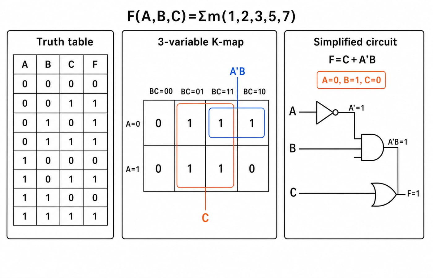
Use the function F(A,B,C)=Sigma m(1,2,3,5,7). A listed minterm produces 1, and every other row produces 0.
A | B | C | Minterm | F |
|---|---|---|---|---|
0 | 0 | 0 | m0 | 0 |
0 | 0 | 1 | m1 | 1 |
0 | 1 | 0 | m2 | 1 |
0 | 1 | 1 | m3 | 1 |
1 | 0 | 0 | m4 | 0 |
1 | 0 | 1 | m5 | 1 |
1 | 1 | 0 | m6 | 0 |
1 | 1 | 1 | m7 | 1 |
The canonical sum of products is:
F=A'B'C + A'BC' + A'BC + AB'C + ABC
Place the values in a three-variable K-map with Gray-order columns BC=00,01,11,10:
BC=00 | BC=01 | BC=11 | BC=10 | |
|---|---|---|---|---|
A=0 | 0 | 1 | 1 | 1 |
A=1 | 0 | 1 | 1 | 0 |
The four-cell group m1,m3,m5,m7 keeps C=1, so it gives C. The two-cell group m2,m3 keeps A=0 and B=1, so it gives A'B. Therefore:
F=C+A'B
For the grouping rules behind that step, use the Boolean algebra and K-map minimisation guide.
At A=0, B=1, C=0, A'=1 and A'B=1, so F=0+1=1, matching row 010. At A=1, B=1, C=0, A'=0 and A'B=0, so F=0, matching row 110.
Why NAND and NOR Are Universal Gates
Copies of a universal gate can construct NOT, AND, and OR, and therefore any Boolean function. NAND supplies all three:
NOT:
A'=NAND(A,A)AND:
A.B=NAND(NAND(A,B),NAND(A,B))OR:
A+B=NAND(NAND(A,A),NAND(B,B))
NOR gives the dual set, with OR now the cheap one:
NOT:
A'=NOR(A,A)OR:
A+B=NOR(NOR(A,B),NOR(A,B))AND:
A.B=NOR(NOR(A,A),NOR(B,B))
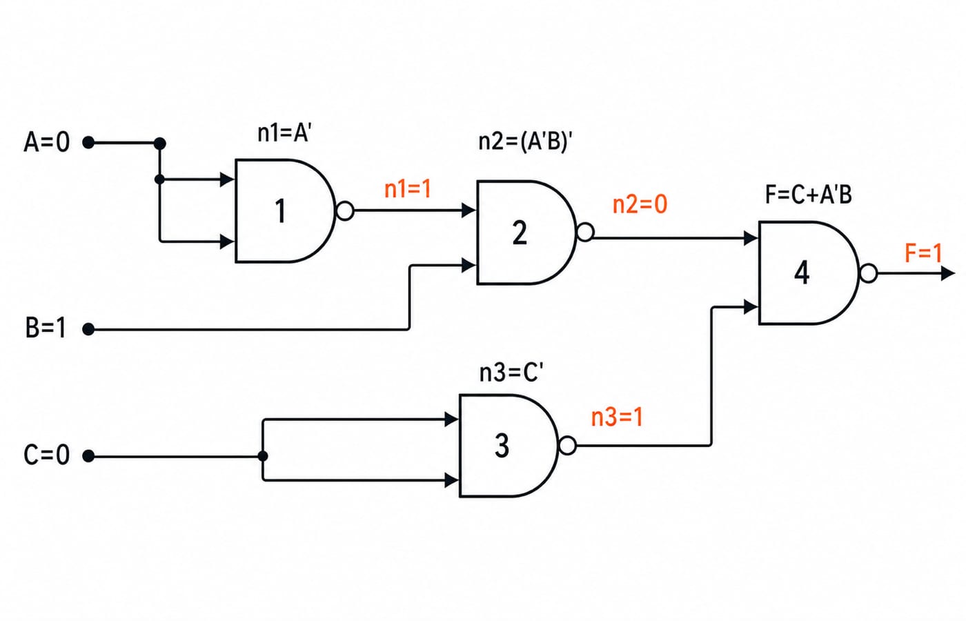
Each of those constructions spends extra gates, so minimise an expression before converting it. Implement F=C+A'B with four NAND gates: n1=NAND(A,A)=A'; n2=NAND(n1,B)=(A'B)'; n3=NAND(C,C)=C'; and F=NAND(n3,n2)=C+A'B by De Morgan's law.
At A=0, B=1, C=0, the signals are n1=1, n2=0, and n3=1. The last gate gives F=NAND(1,0)=1, matching both earlier forms.
Hardware Details That Change the Answer
A small inversion bubble means logical complement. A bubbled output on an AND symbol makes it NAND. A bubbled input is complemented before the gate operation. An active-low label such as RESET_n means the function is asserted when that signal is 0. An AND-shaped gate with input B bubbled and its output bubbled therefore represents Y=(A.B')'.
Propagation delay belongs to a path, not just to the diagram as a whole. Suppose each NAND gate has a worst-case delay of 8 ns. The longest path from A crosses gates 1, 2, and 4, so its bound is 3 x 8 ns = 24 ns. The path from C crosses gates 3 and 4, giving 2 x 8 ns = 16 ns. If A changes at t=10 ns, do not assume F has settled before t=10+24=34 ns on that path.
Fan-in is the number of inputs accepted by a gate. Fan-out describes how many gate inputs one output can drive. Numeric voltage, current, fan-out, and delay limits must come from the named component's data sheet. Finally, a combinational circuit depends on present inputs, while latches, flip-flops, and counters store state and belong to sequential circuit analysis.
Common Logic-Gate Traps and How to Avoid Them
OR versus XOR: At
A=1, B=1, OR produces 1 but XOR produces 0. For two inputs, read XOR as "exactly one input is 1", not "at least one".Incorrect De Morgan conversion:
(A+B)'=A'B', notA'+B';(AB)'=A'+B'. Complement every literal and swap OR with AND. ForA=0, B=1,(0+1)'=0and0'.1'=1.0=0, so both sides agree.Skipped rows or signals: A three-input function requires all eight rows. Write the
000to111scaffold, label every bubble as a complement, and calculate one intermediate signal at a time. Remember thatA'Bmeans(NOT A) AND B, notNOT(AB).
How GATE and Technical Interviews Test Logic Gates
Typical tasks ask you to trace a supplied input vector, identify a gate from its truth table, replace a mixed circuit using only NAND or NOR, simplify before counting gates, or calculate delay along the longest path.
Try a rapid trace: P=NAND(A,B) and Y=XOR(P,C). For A=1, B=1, C=0, P=0 and Y=0. For A=0, B=1, C=1, P=1 and Y=0. Writing P prevents a common mental skip.
To practise these traces against exam-style sets, work through the GATE category and GATE Test Series. Check the current official GATE syllabus or notification before relying on any exam-specific pattern, date, or marking detail.
Logic Gates in One Minute and the Next Step
Translate every symbol into a Boolean expression.
Make all
2^ntruth-table rows in a fixed order.Calculate and label intermediate signals.
Minimise the function before implementing it.
Include inversion bubbles and propagation delay when ideal logic becomes hardware.
Now rebuild F(A,B,C)=Sigma m(1,2,3,5,7) without looking. Verify vectors 010 and 110, then redraw the function using only NAND gates. For structured preparation across the wider syllabus, continue with GATE Guidance by Sanchit Sir.
Keep learning

Functional Completeness in Digital Logic: NAND, NOR and Worked Examples
Learn what makes a Boolean operator set complete, how NAND and NOR recover a standard basis, and how to verify a four-gate NAND construction.
Updated 2 Oct 20266 min readDigital Logic
Boolean Function Counts: Formulas, Worked Examples and Exam Traps
Build the master Boolean-function formula from output choices, then learn how common restrictions change the count through combinations, pairing and inclusion-exclusion.
Updated 27 Sep 20266 min readDigital Logic

Analog-Digital Conversion Basics: ADC, DAC, Worked Examples and Exam Patterns
Build ADC and DAC basics from one consistent transfer model, then practise code selection, reconstruction error, flash and SAR conversion, and bit-depth calculations.
Updated 25 Sep 20266 min readDigital Logic

Universal Realization with NAND and NOR Gates: Concepts, Worked Example and Exam Patterns
Learn why NAND and NOR are universal, then implement one three-variable function using four NAND gates and four NOR gates with verified input traces.
Updated 23 Sep 20265 min readDigital Logic