

Universal Gates: NAND and NOR Truth Tables, Conversions and Worked Examples
Learn why NAND and NOR are functionally complete, then build NOT, AND and OR from each. Two fully traced three-gate circuits make every complement visible.
KnowledgeGate Team
Exam prep & CS education
Updated 1 Nov 20265 min read

Memorising that NAND and NOR are "universal" does not show how either gate can replace NOT, AND and OR. One missed complement can make an entire conversion wrong. Tying a gate's inputs creates NOT; a second homogeneous stage restores AND or OR. For F=A+BC, two complemented first-level signals feed a final NAND; for G=(A+B)C, the dual construction uses NOR. Their eight-row truth tables expose complement and polarity errors before they spread.
NAND and NOR universal gates: meaning, equations and truth tables
A universal, or functionally complete, gate can realise NOT, AND and OR using repeated copies of its type. Those operations build any Boolean function. Multiple physical gates are still required.
Write the defining equations first:
A NAND B = (AB)' = A' + B'A NOR B = (A+B)' = A'B'
De Morgan's law gives the second form. Input complements remain, so NAND is not OR and NOR is not AND.
A | B |
|
|
|
|
|---|---|---|---|---|---|
0 | 0 | 0 | 0 | 1 | 1 |
0 | 1 | 0 | 1 | 1 | 0 |
1 | 0 | 0 | 1 | 1 | 0 |
1 | 1 | 1 | 1 | 0 | 0 |
NAND is 0 only at AB=11; NOR is 1 only at AB=00. Study their wider Digital Logic context in CS Fundamentals for Exams & Placements.
Build NOT, AND and OR using only NAND or only NOR
For NAND-only construction, tie inputs together whenever an inversion is needed:
NOT:
A NAND A = (AA)' = A'.AND: let
X=A NAND B=(AB)'. ThenX NAND X=X'=AB.OR: let
P=A NAND A=A'andQ=B NAND B=B'. ThenP NAND Q=(A'B')'=A+B.
The dual NOR-only constructions are:
NOT:
A NOR A=(A+A)'=A'.OR: let
R=A NOR B=(A+B)'. ThenR NOR R=R'=A+B.AND: let
U=A NOR A=A'andV=B NOR B=B'. ThenU NOR V=(A'+B')'=AB.
At A=1, B=0, the NAND route gives X=1, hence AND is X NAND X=0; P=0,Q=1, hence OR is P NAND Q=1. The NOR route gives R=0, hence OR is R NOR R=1; U=0,V=1, hence AND is U NOR V=0. Both match AND(1,0)=0 and OR(1,0)=1.
NAND-only worked example: implement F(A,B,C)=A+BC
Insert the double complement before drawing gates:
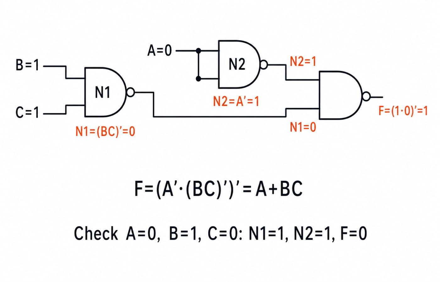
F=A+BC=(A'*(BC)')'
Define N1=B NAND C=(BC)', N2=A NAND A=A', and F=N2 NAND N1. With 2-input gates, this uses exactly three NANDs.
ABC |
|
|
| direct |
|---|---|---|---|---|
000 | 1 | 1 | 0 | 0 |
001 | 1 | 1 | 0 | 0 |
010 | 1 | 1 | 0 | 0 |
011 | 0 | 1 | 1 | 1 |
100 | 1 | 0 | 1 | 1 |
101 | 1 | 0 | 1 | 1 |
110 | 1 | 0 | 1 | 1 |
111 | 0 | 0 | 1 | 1 |
At A=0,B=1,C=1, N1=(1*1)'=0, N2=1, and F=(1*0)'=1. At A=0,B=1,C=0, N1=(1*0)'=1, N2=1, and F=(1*1)'=0. Thus the output vector for ABC=000 through 111 is 0,0,0,1,1,1,1,1.
NOR-only worked example: implement G(A,B,C)=(A+B)C
The expression is in POS form. Complement its factors:
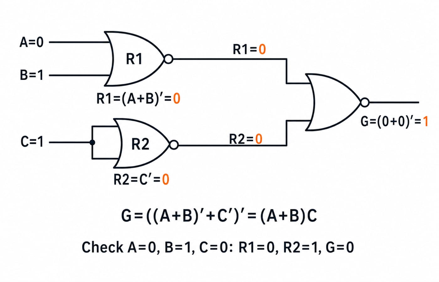
G=(A+B)C=((A+B)' + C')'
Define R1=A NOR B=(A+B)', R2=C NOR C=C', and G=R1 NOR R2. With 2-input gates, this uses exactly three NORs.
ABC |
|
|
| direct |
|---|---|---|---|---|
000 | 1 | 1 | 0 | 0 |
001 | 1 | 0 | 0 | 0 |
010 | 0 | 1 | 0 | 0 |
011 | 0 | 0 | 1 | 1 |
100 | 0 | 1 | 0 | 0 |
101 | 0 | 0 | 1 | 1 |
110 | 0 | 1 | 0 | 0 |
111 | 0 | 0 | 1 | 1 |
At A=0,B=1,C=1, R1=(0+1)'=0, R2=0, and G=(0+0)'=1. At A=0,B=1,C=0, R1=0, R2=1, and G=(0+1)'=0. The output vector is 0,0,0,1,0,1,0,1.
Universal gates implement a Boolean block without changing its function. Universal Realization with NAND and NOR Gates: Concepts, Worked Example and Exam Patterns keeps one Boolean function fixed across both gate families. By contrast, F=A+BC isolates the NAND-SOP path and G=(A+B)C isolates the NOR-POS path, so the complements differ without changing either target function.
NAND-NAND and NOR-NOR conversion patterns without guesswork
The F circuit is the SOP pattern: F=A+BC=(A'*(BC)')'. Its two first-level outputs are A' and (BC)', and the final NAND removes both complements. A one-literal product such as A still needs the tied-input NAND that creates A'.
The G circuit is the POS dual: G=(A+B)C=((A+B)'+C')'. Its first-level outputs are (A+B)' and C', and the final NOR removes both complements. These concrete signals explain why NAND-NAND suits SOP and NOR-NOR suits POS.
General bubble-pushing, fan-in assumptions, XOR/XNOR networks and minimum counts are developed in Universal Gates for GATE: NAND, NOR and Minimum Gate Counts. Simplify first; minimum terms do not guarantee minimum gate cost, which also depends on fan-in, available complements and reusable nodes.
Universal-gate traps and the repair for each
tempting move | what goes wrong | repair |
|---|---|---|
Read | Input complements disappear | Write |
Ignore tied inputs | You miss | Simplify tied inputs first |
Drop the outer complement in | You get | Mark the final output complement |
Mix NAND-NAND SOP with NOR-NOR POS | The levels implement another expression | Identify SOP or POS first |
Check only one row | A wrong circuit may pass it | Compare every row with the original |
Claim a minimum without assumptions | Fan-in and supplied complements change cost | State inputs, supplied signals and reuse |
Check polarity: at A=1,B=1, NAND gives 0 while OR gives 1. At A=0,B=0, NOR gives 1 while AND gives 0.
Label intermediate wires, substitute left to right, then compare with the original. One differing row disproves equivalence.
How exam-style questions test NAND and NOR
NAND and NOR may be tested through output vectors, gate substitutions, intermediate values and gate-count analysis; current exam patterns should be checked against the official notification.
Output vector
1,1,1,0identifies NAND;1,0,0,0identifies NOR.OR is
(A NAND A) NAND (B NAND B).AND is
(A NOR A) NOR (B NOR B).For the NAND network at
ABC=011,N1=0,N2=1,F=1.For the NOR network at
ABC=101,R1=0,R2=0,G=1.With 2-input gates, the F and G circuits each use three gates: two first-level complements and one final homogeneous gate. Changing fan-in or supplying complements can change the count.
Write intermediate values so errors stay visible. Use GATE Test Series, Mocks and Topic-wise Tests for timed practice.
Universal gates: the short version and next step
Recall these relationships:
NAND is
(AB)'.NOR is
(A+B)'.Tying a gate's inputs makes NOT.
NAND-NAND suits SOP.
NOR-NOR suits POS.
A full truth-table match proves equivalence.
Without looking, redraw both three-gate networks. Calculate N1,N2,F and R1,R2,G at ABC=011 and 010. The expected final pairs are F: 1,0 and G: 1,0.
For broader learning in Digital Electronics and Logic Gates & Hardware, continue with Zero to Hero, Complete CS Course.
Go deeper with the full courseDigital Electronics
Keep learning

Universal Gates for GATE: Realizing Any Function with Only NAND or Only NOR, and Counting the Minimum Gates
Turn SOP into NAND-only and POS into NOR-only circuits, count every gate, and learn the exact two-input counts for AND, OR, XOR and XNOR.
Updated 30 Oct 20266 min read191 viewsDigital Logic

Universal Realization with NAND and NOR Gates: Concepts, Worked Example and Exam Patterns
Learn why NAND and NOR are universal, then implement one three-variable function using four NAND gates and four NOR gates with verified input traces.
Updated 23 Sep 20265 min read83 viewsDigital Logic

NAND and NOR Universal Gates MCQs: 12 Solved Questions with Explanations
Solve 12 NAND and NOR universal-gate MCQs in order, from gate identification to functional completeness. Each answer shows the Boolean step that decides the option.
Updated 29 Oct 20268 min read82 viewsDigital Electronics MCQs

Universal Realization MCQs: 12 Solved NAND and NOR Questions
Solve 12 universal realization MCQs in a rising sequence, from identifying universal gates to minimising NAND and NOR networks and tracing multi-level circuits.
Updated 30 Aug 20267 min read163 viewsDigital Electronics MCQs