

Digital Logic Semester Guide: Number Systems, K-Maps, Circuits and Timing
Build Digital Logic as one connected workflow. Follow complete examples and checkpoints covering number representation, circuits, state and timing.
KnowledgeGate Team
Exam prep & CS education
Updated 3 Nov 20266 min read
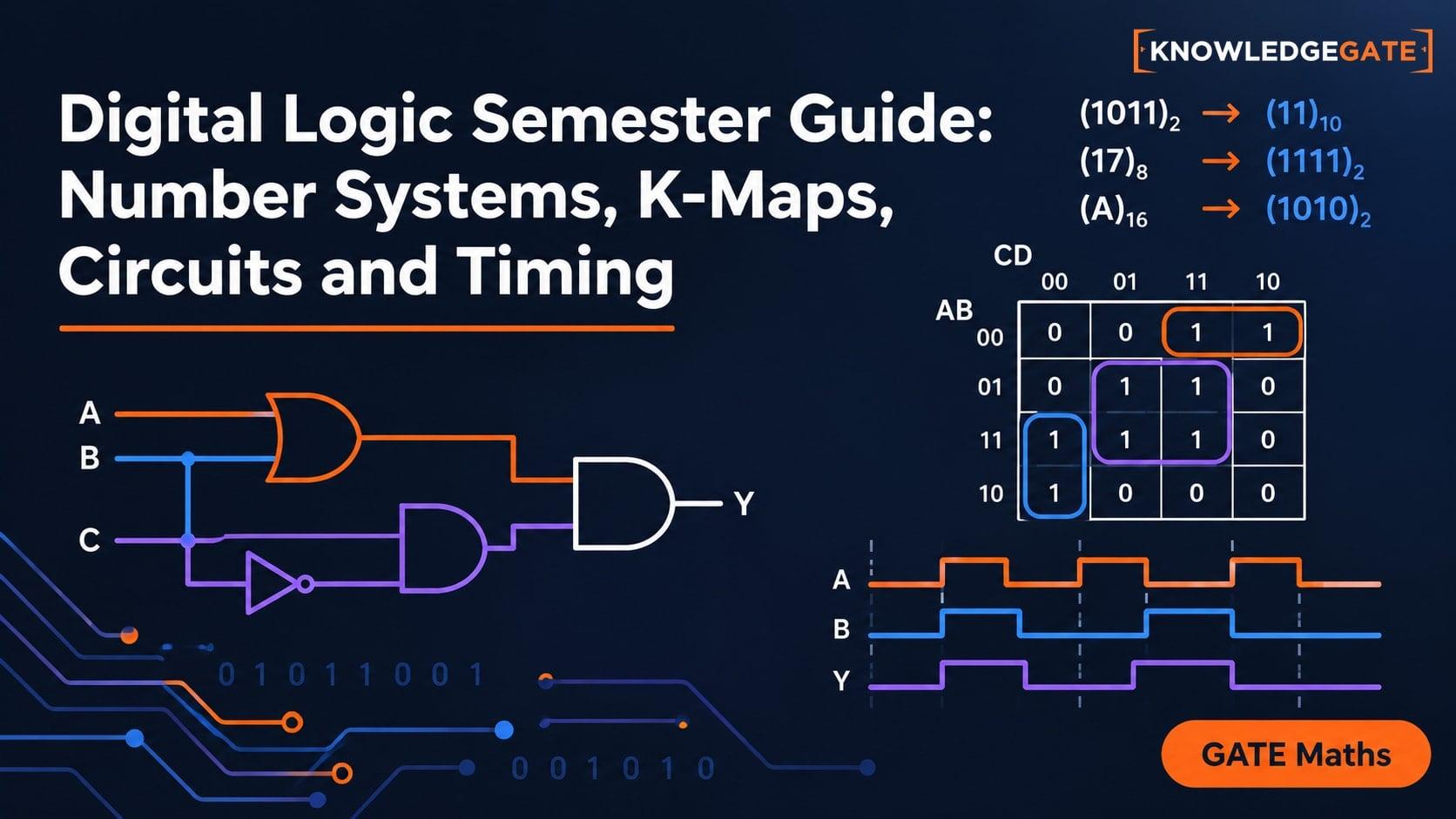
Digital Logic links representation to Boolean algebra, K-Maps, circuit blocks, stored state and timing. A student who can convert a value but cannot trace a carry or clock edge needs those dependencies in order. The dependency is visible in one worked sequence: values are converted, a four-variable function is minimised, an adder is traced, a custom state sequence is followed and setup timing is checked.
Place Digital Logic within the CS Fundamentals map before you begin.
1. Build the Digital Logic dependency map before studying chapters
Study in this order: number systems and signed representation -> Boolean laws and gates -> SOP/POS forms -> K-Map minimisation -> combinational blocks -> latches and flip-flops -> counters/registers -> setup, hold and propagation timing.
Representation gives meaning to a bit pattern, Boolean laws create the expression, and K-Maps minimise it. Combinational blocks operate on present inputs; stored state adds clock edges and timing limits.
Keep the two circuit families separate. For combinational logic, the present output depends on present inputs: Y=f(X). For sequential logic, the next output also depends on stored state: Q_next=f(Q_current,X). An edge-triggered circuit observes state changes at its active clock edge.
2. Number systems and signed values: calculate before memorising rules
Convert 45_10 by place value first:
45 = 32 + 8 + 4 + 1 = 2^5 + 2^3 + 2^2 + 2^0
Those occupied positions give 101101_2. Regroup from the right as 101 101; each group is 5, so the octal form is 55_8. For hexadecimal, pad on the left and group as 0010 1101, which gives 2D_16. Therefore:
45_10=101101_2=55_8=2D_16
Now represent -13 in 8-bit two's complement. Start with +13=00001101, invert every bit to get 11110010, then add 1:
11110010 + 1 = 11110011
As an unsigned value, 11110011 is 128+64+32+16+2+1=243; under 8-bit two's complement, its value is 243-256=-13.
These bits are 243 unsigned and -13 signed in 8-bit two's complement; declare base, width and convention before arithmetic.
3. Fully worked K-Map: turn eight minterms into two product terms
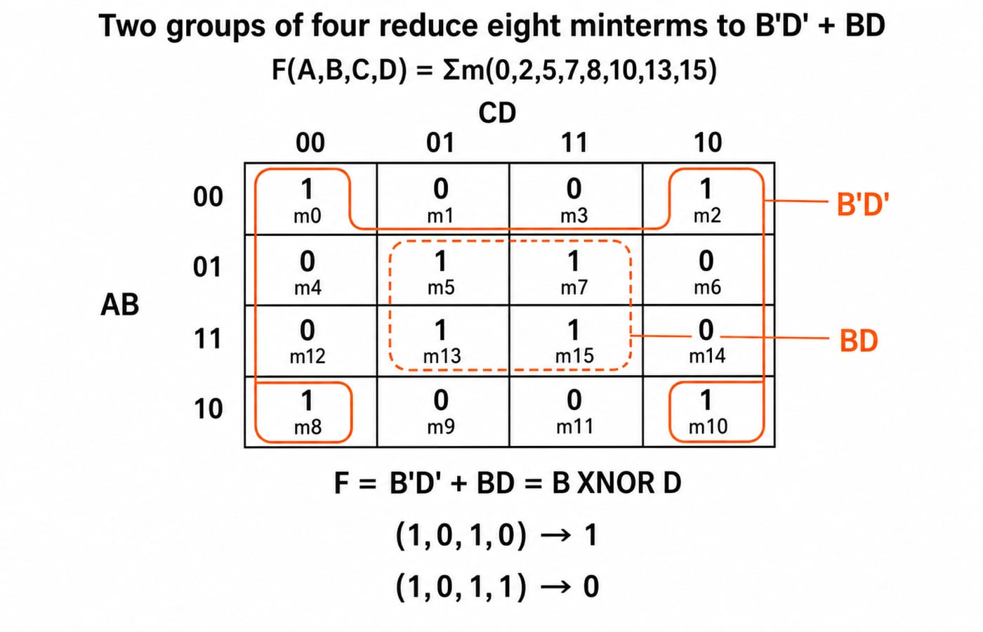
Take F(A,B,C,D)=Sigma m(0,2,5,7,8,10,13,15). Use Gray-code rows AB=00,01,11,10 and Gray-code columns CD=00,01,11,10. Every minterm not listed is 0.
|
|
|
|
|
|---|---|---|---|---|
| 1 | 0 | 0 | 1 |
| 0 | 1 | 1 | 0 |
| 0 | 1 | 1 | 0 |
| 1 | 0 | 0 | 1 |
The four corners {m0,m2,m8,m10} are adjacent through wrap-around. Across that group, A and C vary while B=0 and D=0 remain fixed, so the term is B'D'. The centre group {m5,m7,m13,m15} keeps B=1 and D=1, producing BD.
Therefore F=B'D'+BD. This is B XNOR D, independent of A and C. For (A,B,C,D)=(1,0,1,0), B'D'=1 and BD=0, so F=1. For (1,0,1,1), both terms are 0, so F=0.
Implement it with one XNOR or two AND gates and an OR gate, inverting B and D for B'D'. See Boolean Algebra and K-Map Minimization for fuller grouping.
4. Combinational design: trace data and carry through real blocks
Add A=1101_2 (13_10) and B=0011_2 (3_10) with input carry C0=0. Trace from the least significant bit:
Bit 0:
1+1+0 -> S0=0,C1=1Bit 1:
0+1+1 -> S1=0,C2=1Bit 2:
1+0+1 -> S2=0,C3=1Bit 3:
1+0+1 -> S3=0,C4=1
Reading the final carry followed by the sum bits gives C4S3S2S1S0=10000_2=16_10, matching 13+3=16.
Now implement G(A,B,C)=Sigma m(0,3,4,7) on a 4-to-1 MUX with A,B as its select lines. Hold each select combination fixed and inspect how the output depends on C: AB=00 gives I0=C'; AB=01 gives I1=C; AB=10 gives I2=C'; and AB=11 gives I3=C.
Check inputs: ABC=001 selects I0=C'=1; ABC=110 selects I3=C=0. The adder shows carry propagation; the MUX reduces a three-variable function to four data inputs.
5. Sequential circuits: make state changes explicit at every edge
A latch is level-sensitive. The state trace below uses edge-triggered D flip-flops, so all bits sample their next values on the same active clock edge and hold between edges.
Use three D flip-flops with the specified cycle 000 -> 011 -> 101 -> 110 -> 000. At each active edge, D2D1D0 equals the listed next state. Starting at 000, edges 1, 2, 3 and 4 produce 011, 101, 110, and 000. All three flip-flops receive the same clock edge, so the state sequence is synchronous.
The earlier Sequential Circuits: Flip-Flops and Counters guide owns the full characteristic tables and its worked 2-bit Mod-4 design; this post uses a different state cycle to connect state notation with the semester sequence and the timing check.
6. Timing analysis: calculate margins, minimum period, and failure
Use four quantities. t_setup is the stable time required before the sampling edge, while t_hold is the stable time required after it. t_clk-to-Q is the delay from the edge to the launching output. t_comb(max) is the maximum intervening logic delay.
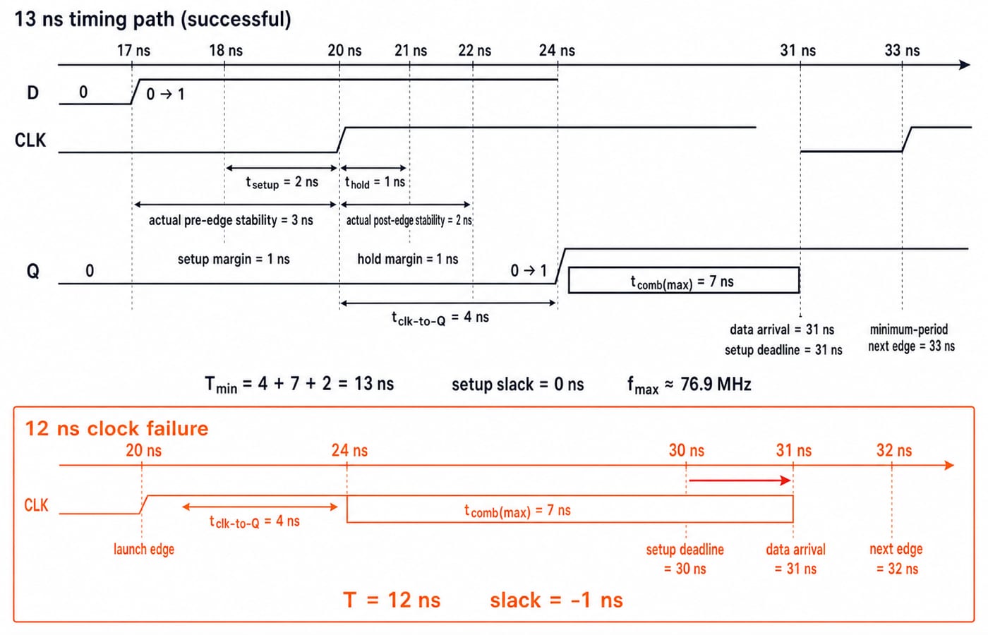
Suppose D changes from 0 to 1 at t=17 ns, a positive edge occurs at t=20 ns, and D stays stable through t=22 ns. With t_setup=2 ns, pre-edge stability is 20-17=3 ns, so setup margin is 3-2=1 ns. With t_hold=1 ns, post-edge stability is 22-20=2 ns, so hold margin is 2-1=1 ns. Both pass. If t_clk-to-Q=4 ns, Q becomes 1 at t=24 ns.
For the path to a second register, let t_comb(max)=7 ns, destination t_setup=2 ns, and skew and jitter be zero. Data arrives at 24+7=31 ns. The minimum clock period is:
T_min = 4+7+2 = 13 ns
Thus f_max=1/(13 ns), approximately 76.9 MHz. The next edge after 20 ns is 33 ns, with setup deadline 33-2=31 ns. Arrival at 31 ns gives zero setup slack.
At a 12 ns period, the deadline is 30 ns while data arrives at 31 ns, so setup fails by 1 ns. This maximum-delay check does not prove hold at the second register; use a minimum-delay check separately.
7. How semester questions expose weak links, plus the exact corrections
Questions test representation, minimisation, circuit tracing and timing.
Confirm the current syllabus, unit coverage, paper format, and instructions on your university's official website. The forms here are study patterns, not claims about a particular university paper.
Correct these traps:
Binary K-Map row order: use Gray order
00,01,11,10.Groups cannot cross an edge: the four corners are adjacent by wrap-around.
Diagonal grouping: valid groups are rectangular and contain a power-of-two number of cells.
11110011always means-13: only with 8-bit two's-complement interpretation.A counter changes continuously: these flip-flops update on the active edge.
A slower clock fixes all timing: it can help setup, but hold needs a minimum-delay check.
Check yourself: 58_10=111010_2; the K-Map function is 0 when B=1,D=0; 1101_2+0011_2=10000_2; three edges from 000 lead to 110; and t_clk-to-Q=3 ns, t_comb(max)=8 ns, t_setup=2 ns give T_min=13 ns and f_max approximately 76.9 MHz. For extra drills, KnowledgeGate has about 1,600 published Digital Electronics practice questions. The practice-pool count is not an official exam statistic and will change.
8. Digital Logic semester guide: the short version and next step
Represent the value correctly, express the logic, minimise it, select a combinational implementation, add state only when past behaviour matters, then prove the clock leaves enough time. The central results are 45_10=101101_2, F=B'D'+BD, 1101_2+0011_2=10000_2, the state cycle 000,011,101,110, and T_min=13 ns.
Use Digital Electronics for the focused continuation or Zero to Hero for a broader multi-subject semester route. Next, redraw the K-Map and timing line from memory, then check every value against sections 3 and 6.
Go deeper with the full courseDigital Electronics
Keep learning

RSSB Computer Instructor Digital Logic and Computer Fundamentals: Worked Number Systems, Boolean Algebra and Memory Basics
Connect number systems, Boolean algebra, memory capacity and CPU organisation through four checked examples designed for RSSB Computer Instructor preparation.
Updated 25 Aug 20266 min readDigital Logic

Adders and Subtractors in Digital Logic: Circuits, Worked Examples and Exam Traps
Learn adders and subtractors from one-bit truth tables to four-bit ripple circuits, with verified addition, subtraction, overflow and delay examples.
Updated 26 Aug 20266 min readDigital Logic

Number System MCQs: 12 solved digital electronics questions with explanations
Number system MCQs with solutions: 12 solved GATE questions on binary, octal and hex conversion, radix equations, and 1's and 2's complement signed numbers.
Updated 30 Oct 20266 min read408 viewsDigital Electronics MCQs

Boolean Minimization in Digital Electronics: Laws, K-Maps and Worked Examples
Learn to reduce Boolean expressions with auditable algebra, legal K-map groups, don't-cares, and truth-table checks. Includes complete SOP and POS examples.
Updated 30 Oct 20267 min read80 viewsDigital Logic