

Sequential Logic and Latches Explained: SR and D Latches with Worked Timing Examples
Learn how feedback creates stored state, how NOR and NAND SR latches differ, and how to solve a gated D-latch timing trace interval by interval.
KnowledgeGate Team
Exam prep & CS education
Updated 31 Oct 20266 min read
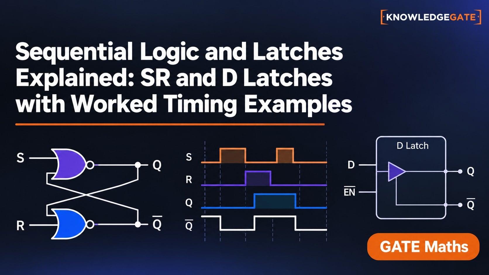
A truth table is enough when a circuit's output depends only on its current input. It is not enough when the answer also depends on what happened one instant earlier. Sequential logic adds state to ordinary logic. An SR latch introduces state storage, a D latch resolves the SR latch's conflicting-input problem, and timing traces are calculated interval by interval.
Sequential logic adds state to ordinary logic
A combinational circuit follows a relation such as Y(t) = G(X(t)). Give it the same current input and it produces the same output. A sequential circuit instead follows Q(n+1) = F(X(n), Q(n)). Here, Q(n) is the stored present state, while Q(n+1) is the next state produced from both the input and that stored context.
For example, if X=0, an inverter must output 1. A storage element given an input of 0 may still hold either Q=0 or Q=1, depending on its earlier state and control inputs. Feedback makes this possible. Part of the circuit's output is returned to its input network, so the value already stored can influence the value stored next.
The cross-coupled NOR SR latch, one row at a time
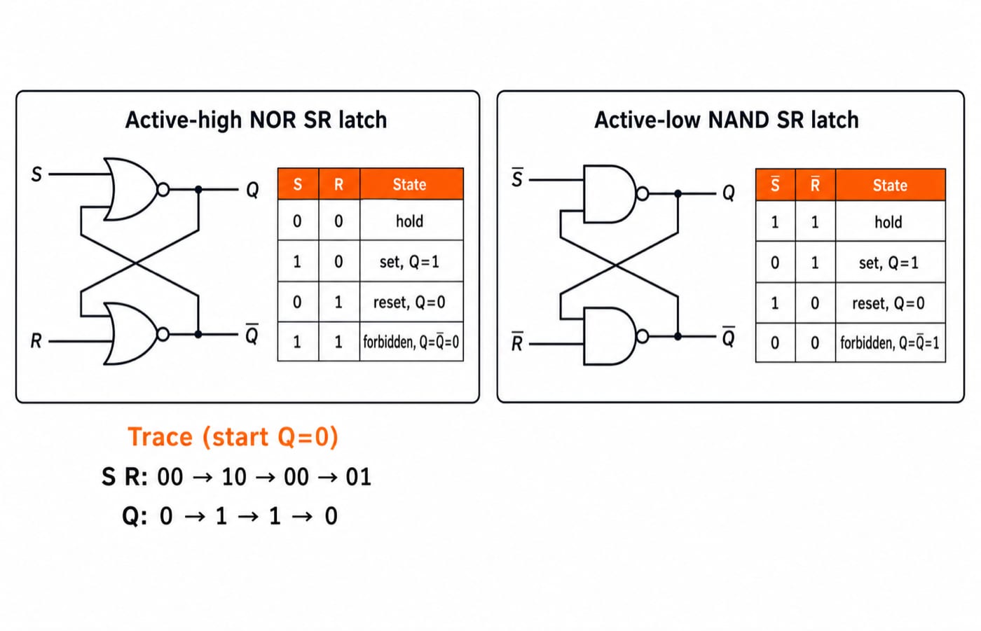
An active-high SR latch uses two cross-coupled NOR gates. S requests set, R requests reset, and the normal outputs are complements, Q and Q-bar.
S | R | Next Q | Meaning |
|---|---|---|---|
0 | 0 | Previous Q | Hold |
1 | 0 | 1 | Set |
0 | 1 | 0 | Reset |
1 | 1 | Forbidden | Both outputs become 0 |
For valid inputs, the active-high SR latch has Q(n+1) = S + R-bar.Q(n), with S.R = 0 excluding the forbidden row. The hold row is often misread. Starting with Q=0, apply (S,R) = (0,0), (1,0), (0,0), (0,1). The resulting values are Q = 0, 1, 1, 0. The first 00 preserves 0, but the second 00 preserves 1. Hold does not mean reset.
For S=R=1, both NOR outputs are forced to 0, so Q and Q-bar are no longer complementary. On release to 00, small gate-delay differences may choose the surviving state. This row is therefore forbidden.
Active-low NAND contrast: A NAND SR latch reverses the active levels. For
(S-bar,R-bar),11holds,01setsQ=1,10resetsQ=0, and00is forbidden withQ=Q-bar=1. Check bubbles or overbars before choosing a table.
The gated D latch removes the conflicting input choice
An active-high gated D latch starts from the SR idea but generates the two requests from one data input. Its effective inputs are S=E.D and R=E.D-bar. When enable E=1, the SR stage receives S=D and R=D-bar. They cannot both be 1. When E=0, both effective inputs are 0, so the latch holds.
Its rule is compact: E=0 gives Q(n+1)=Q(n), while E=1 gives Q(n+1)=D. Combining the cases gives the characteristic equation Q(n+1) = E.D + E-bar.Q(n). The first term passes data while enabled, and the second preserves the present state while disabled. The latch is called transparent while enabled because changes at D can pass to Q throughout the active level, after the circuit's propagation delay. It is not waiting for an edge.
Worked timing example: calculate every D-latch interval
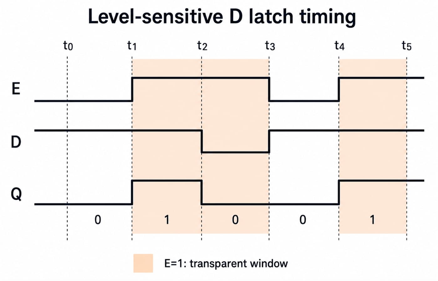
Take Q(t0-) = 0. Divide the waveform wherever E or D changes, then apply Q(next) = E.D + E-bar.Q(present) chronologically.
Interval | E | D | Present Q | Calculation | Stored Q |
|---|---|---|---|---|---|
| 0 | 1 | 0 |
| 0 |
| 1 | 1 | 0 |
| 1 |
| 1 | 0 | 1 |
| 0 |
| 0 | 1 | 0 |
| 0 |
| 1 | 1 | 0 |
| 1 |
The stored levels are therefore Q = 0, 1, 0, 0, 1. Interval 1 holds the initial 0 even though D=1, because enable is low. In interval 2, enable goes high, so the latch becomes transparent and Q takes the current D=1. While enable remains high in interval 3, D changes to 0, and Q follows it.
At t3, D changes from 0 to 1, but E=0 for the following interval. The stored output therefore remains 0. At t4, enable returns to 1, so D=1 passes through and the final level becomes 1. A physical output changes after a propagation delay, but no numerical delay is needed here.
Latch versus flip-flop: level sensitivity is the deciding test
A latch is level-sensitive. It can respond throughout the interval in which its enable is active, in the ideal logic model. A flip-flop is edge-triggered. It samples its input only at a specified transition, such as a rising edge.
In the worked waveform, the D latch follows D at both t1 and t2 because E stays high across that period. A positive-edge-triggered D flip-flop would sample D=1 at the rising edge at t1, then ignore the change to D=0 at t2. It would wait for the next rising edge at t4.
Two latches controlled on opposite phases can form a master-slave storage element. One phase accepts data while the other isolates the output, producing edge-like external behaviour. For latch polarity and level-sensitive timing, use the SR and D traces above. For flip-flop tables, excitation, and counter design, continue with Sequential Circuits, Flip-Flops and Counters.
Traps that make otherwise correct latch answers fail
Treating
00as reset in an active-high NOR latch. It is hold. Reset isS=0,R=1.Copying the NOR table to an active-low NAND latch. Look for input bubbles or overbars first, then select the correct polarity.
Updating a latch only at an edge. While enable is active, a D latch is transparent and may follow more than one data change.
Using the new
Qtoo early in a trace. Write the present state, apply the truth-table row or characteristic equation, and only then record the next state.Giving the forbidden row a stable logical meaning. Explain that complementary outputs are violated. Do not predict the state after release unless the circuit supplies gate-delay or priority information.
These checks separate a clean state trace from a memorised table used with the wrong convention.
How exam questions turn the same idea into different formats
The same core idea usually appears in four forms: completing an SR or D truth table, tracing Q across an enable or clock waveform, deriving or applying a characteristic equation, and converting one flip-flop form into another from its excitation requirements.
For a waveform, reuse the 0, 1, 0, 0, 1 method: identify the active level, mark the initial state, divide the signal into intervals, calculate chronologically, and inspect every held interval. For the conversion branch, use Flip-Flop Conversion and Excitation Tables for GATE to connect required transitions with input equations. Then use the sequential-logic and latch practice questions to test polarity, timing, and state tracking rather than only rereading definitions.
Short version and the next useful step
Sequential logic needs a present state. An SR latch stores it through feedback. A D latch prevents conflicting normal inputs. Its timing is solved interval by interval, not edge by edge.
For structured subject teaching, continue with GATE Guidance by Sanchit Sir. When you are ready to test timing and state questions, use the GATE Test Series. To compare the wider preparation route, start from the GATE CS Exam category.
Go deeper with the full courseDigital Electronics
Keep learning

Sequential Logic and Latches MCQs: 10 Solved Questions with Explanations
Solve 10 published-bank questions on sequential logic, latch polarity, state transitions and multivibrators. Each answer explains the decision that gets you to the next state.
Updated 30 Oct 20267 min readDigital Electronics MCQs

Sequential circuits: flip-flops, latches and counters explained
Sequential circuits for GATE: SR, D, JK and T flip-flops, excitation tables, latch versus flip-flop, and a fully worked synchronous counter design example.
Updated 30 Oct 20265 min read87 viewsDigital Logic
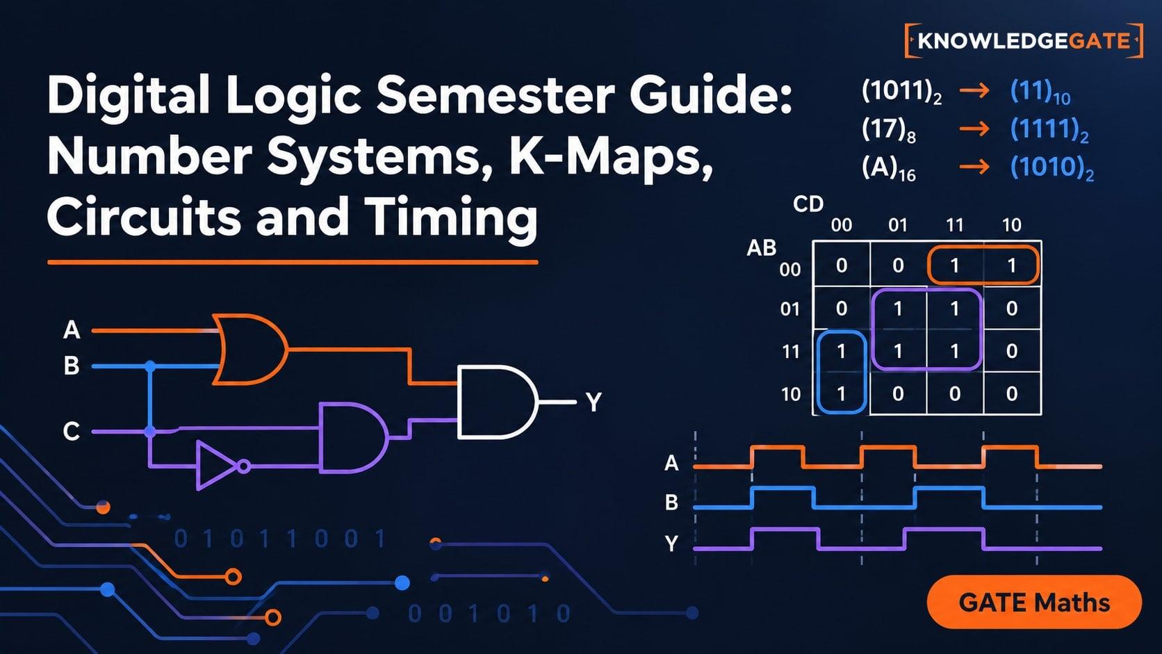
Digital Logic Semester Guide: Number Systems, K-Maps, Circuits and Timing
Build Digital Logic as one connected workflow. Follow complete examples and checkpoints covering number representation, circuits, state and timing.
Updated 3 Nov 20266 min readDigital Logic

Flip-Flop Conversion for GATE: Excitation Tables and the SR, JK, D, T Conversion Recipe, Solved
Convert one flip-flop into another with the target transition, the available device's excitation table and a K-map. The solved JK-to-T case shows every row.
Updated 30 Oct 20266 min read125 viewsDigital Logic