Special Logic Circuits: ROM, Majority Logic and Array Multiplier Examples
Learn one method for analysing special logic circuits, then apply it to majority logic, a BCD detector, programmable logic and two versions of a 4-bit multiplier.
KnowledgeGate Team
Exam prep & CS education
Updated 22 Sep 20266 min read
Special logic circuits can feel like a miscellaneous list because majority voters, code detectors, ROMs, PLAs and multipliers do not share one familiar symbol. The reliable method is to identify the input-output mapping, write its Boolean or word-level function, and then choose or analyse the hardware. Logic Circuit Analysis: Boolean Simplification and Worked Examples owns node-by-node tracing of connected gate diagrams; the circuits below apply that method to majority voting, BCD detection, programmable logic and multiplication.
Special logic circuits: the common combinational idea
A combinational circuit has no stored state. Each output depends only on current inputs, not on clock history or an earlier input. The word "special" is only a teaching bucket for useful mappings built from familiar gates or regular structures, not a different class of logic.
Circuit group | Typical purpose | Signature relation or idea |
|---|---|---|
Decision circuits | Majority, parity and comparison decisions |
|
Code circuits | Detect or convert coded patterns | For three data bits, the even-parity bit is |
Programmable logic | Implement a truth table or sum-of-products functions | An |
Arithmetic arrays | Form and combine regular partial products | An unsigned multiplier computes |
Multiplexers, decoders and ordinary adders remain reusable building blocks. Each circuit below is justified from its input-output relation rather than treated as a memorised symbol.
Majority logic: truth table, Boolean form and MUX realisation
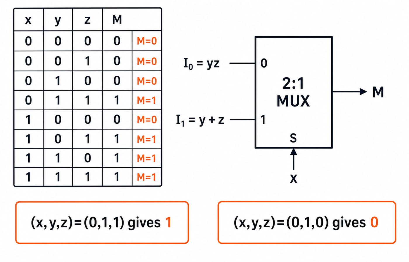
For three inputs, the majority output M is 1 when at least two of x, y and z are 1. Grouping the truth-table rows gives:
000, 001, 010, 100 -> M=0011, 101, 110, 111 -> M=1
There are three ways to select a pair of 1s, so the Boolean function is M = xy + xz + yz.
The earlier Digital Fundamentals and Boolean Algebra Explained derives the same majority expression with Boolean laws and verifies all eight rows. Here the expression becomes a 2:1 MUX realisation.
Now use a 2:1 MUX with select x. For x=0, M=yz, so I0=yz. For x=1, M=y+z, so I1=y+z. The MUX evaluates M=x'yz+x(y+z), equivalent to the majority expression.
Check actual inputs. For (x,y,z)=(0,1,1), the MUX selects I0=1x1=1. For (1,0,1), it selects I1=0+1=1. For (0,1,0), it selects I0=1x0=0.
Majority is not XOR. Majority asks whether the number of 1s reaches a threshold, while XOR reports odd parity. Both happen to produce 1 for 111, but for 001, XOR is 1 and majority is 0. One matching row cannot make the functions equivalent.
Code detector worked example: flag BCD digits 5 through 9
Let A B C D be the 8, 4, 2 and 1 bits of a valid 8421 BCD digit. We want F=1 for decimal 5, 6, 7, 8 and 9, so F = Sum m(5,6,7,8,9). Codes 10 through 15 can be treated as don't-cares because the stated input domain contains only valid BCD digits.
Digit encoding, correction arithmetic and Gray-code conversion are separate tasks. This detector instead maps valid 8421 inputs to one threshold output.
Minimisation gives F = A + B(C + D). The A term covers valid digits 8 and 9. When A=0 and B=1, the factor C+D separates 5, 6 and 7 from digit 4. The hardware needs three gates: one OR gate for C+D, one AND gate with B, and one final OR gate with A.
Boundary checks make the result clear:
Decimal 4 is
0100, soF=0+1(0+0)=0.Decimal 5 is
0101, soF=0+1(0+1)=1.Decimal 9 is
1001, soF=1+0(0+1)=1.
Binary codes 1010 through 1111 are invalid BCD inputs here. They are not extra decimal digits whose outputs were specified.
ROM implementation of a 4-bit multiplier
An n-input, m-output combinational mapping needs 2^n ROM words of m bits each. Its size is 2^n x m, totalling 2^n x m bits. The input selects an address, and the stored word is the output.
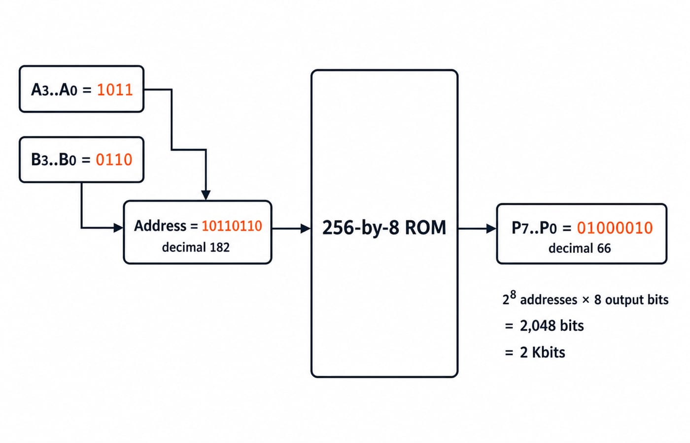
Two unsigned 4-bit operands supply 4+4=8 address bits. That means 2^8=256 addresses, not eight addresses. The maximum input value is 15, and 15x15=225=11100001 in binary, so the product needs 8 bits. The complete ROM is therefore 256 x 8 = 2,048 bits = 2 Kbits.
Take A=1011 in binary, which is 11, and B=0110, which is 6. If the address concatenates A followed by B, the address is 10110110, or 128+32+16+4+2=182. Word 182 stores 11x6=66=01000010 in binary. The two common traps are allocating only eight words because there are eight address bits, and keeping only four output bits even though the product can require eight.
The earlier Adders and Subtractors in Digital Logic uses 1011 and 0110 to trace addition and carry. Here the same operands index a ROM and generate shifted partial products: their product is 66, not the earlier sum 17.
ROM, PLA and PAL: what is actually programmable
Device | AND side | OR side |
|---|---|---|
ROM | Fixed decoder or AND plane generates all minterms | Programmed output connections select the required minterms |
PLA | Programmable | Programmable |
PAL | Programmable | Fixed structure |
Consider F1=A'B+AC and F2=AB'+AC. A PLA forms the three distinct product terms A'B, AB' and AC, then sends the shared AC term to both outputs. A ROM sees three input bits and two output bits, so its size is 2^3 x 2 = 8 x 2 = 16 bits, regardless of how few terms appear in the simplified equations.
A ROM is direct for an arbitrary truth table. A PLA suits shared product terms. PAL feasibility depends on the available OR inputs and product terms per output. No device is universally the smallest.
Array multiplier: reach the same product through partial products
Reuse A=1011=11 and B=0110=6 to cross-check the ROM result. Since B has bits b3b2b1b0=0110, the four 8-bit shifted partial-product rows are:
b0=0: 00000000
b1=1: 00010110
b2=1: 00101100
b3=0: 00000000
       --------
sum:   01000010
The nonzero rows represent 11x2=22 and 11x4=44. Their sum is 22+44=66, which is 01000010 in binary, exactly the word stored by the ROM.
An n x n array multiplier forms n^2 one-bit partial products with AND operations. A 4-bit design therefore contains 16 such partial products even though this particular input produces only two nonzero shifted rows. The regular adder array combines the rows. With constant gate delay, a standard ripple-style array multiplier has a critical path through O(n) adder stages, so its delay is Theta(n). The Theta(n^2) scale belongs to partial-product hardware, not the critical-path delay.
Special logic circuit exam patterns and traps
Questions on this topic usually ask you to derive a majority or parity function, count satisfying input assignments, minimise a code detector with valid don't-cares, size a ROM from its address and word widths, or distinguish multiplier hardware from delay.
Common traps to check:
A ROM size must distinguish words from total bits.
Two unsigned
n-bit operands may need a2n-bit product.Majority tests a threshold; XOR tests parity.
Invalid BCD codes may be don't-cares only when the input specification permits it.
An array multiplier has
n^2partial products, but a standard ripple-style design hasTheta(n)delay.
Use the GATE CS Exam category to place ROM sizing, code detectors and multiplier timing within a broader preparation route.
Special logic circuits: the short version and next step
Keep five results ready for retrieval: M=xy+xz+yz; a 2^n x m ROM stores 2^n x m bits; the 4-bit multiplier needs 256 x 8 = 2,048 bits; a standard array multiplier forms n^2 partial products but has Theta(n) critical-path delay; and a PLA can share product terms across outputs.
Now redraw the majority MUX, recompute the BCD detector for digits 4, 5 and 9, and reproduce 11x6=66 through both ROM lookup and partial-product addition. For sequenced Digital Electronics study and practice, continue with GATE Guidance by Sanchit Sir.
Keep learning

Functional Completeness in Digital Logic: NAND, NOR and Worked Examples
Learn what makes a Boolean operator set complete, how NAND and NOR recover a standard basis, and how to verify a four-gate NAND construction.
Updated 2 Oct 20266 min readDigital Logic
Boolean Function Counts: Formulas, Worked Examples and Exam Traps
Build the master Boolean-function formula from output choices, then learn how common restrictions change the count through combinations, pairing and inclusion-exclusion.
Updated 27 Sep 20266 min readDigital Logic

Analog-Digital Conversion Basics: ADC, DAC, Worked Examples and Exam Patterns
Build ADC and DAC basics from one consistent transfer model, then practise code selection, reconstruction error, flash and SAR conversion, and bit-depth calculations.
Updated 25 Sep 20266 min readDigital Logic

Universal Realization with NAND and NOR Gates: Concepts, Worked Example and Exam Patterns
Learn why NAND and NOR are universal, then implement one three-variable function using four NAND gates and four NOR gates with verified input traces.
Updated 23 Sep 20265 min readDigital Logic