Combinational Circuits in Digital Electronics: Design, MUX, Decoders and Worked Examples
Learn a repeatable method for converting a logic specification into a verified combinational circuit, then apply it to adders, multiplexers, decoders, parity and hazards.
KnowledgeGate Team
Exam prep & CS education
Updated 2 Aug 20266 min read86 views

Students often memorise the symbols for a multiplexer, decoder and adder, yet get stuck when a word problem must become a truth table and then a circuit. One sequence closes that gap: specification, truth table, canonical expression, minimisation, device choice, verification. It runs the same way whether the answer turns out to be an adder, a multiplexer, a decoder or a parity checker. It assumes you can already handle Boolean algebra and K-map minimisation, which supplies the minimisation step, and it carries straight into GATE CS preparation, where a question usually hands you one step and asks for the next.
What makes a circuit combinational?
A combinational circuit's outputs are Boolean functions of the present input vector: Y = f(X). It stores no state and needs no clock. Sequential logic also depends on stored past state.
Circuit | Input to output function |
|---|---|
Adder | Two or three input bits to sum and carry |
Multiplexer | Many data inputs to one selected output |
Decoder | An n-bit code to one of up to 2^n asserted outputs |
Comparator | Two binary words to greater, equal and less outputs |
Parity circuit | Data bits to a parity bit or check result |
Real gates still have propagation delay. Unequal path delays can produce a brief glitch even though the Boolean model is memoryless.
The six-step design method and a majority circuit
Use the same sequence for any combinational design:
Translate the verbal specification and name every input and output.
Build the complete truth table.
Write a canonical SOP or POS expression.
Minimise the expression.
Choose and draw an implementation.
Verify representative rows and boundary cases.
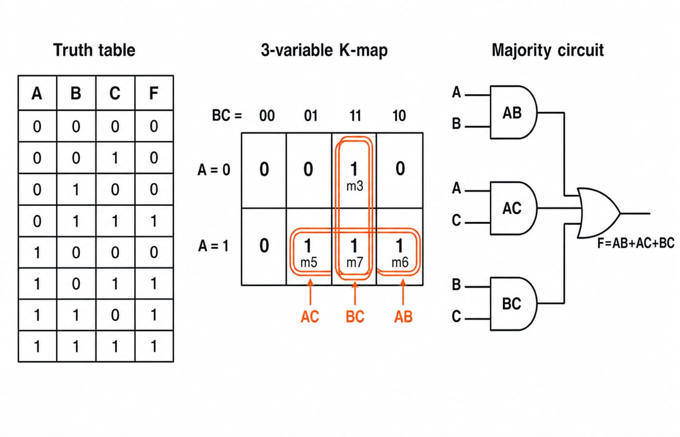
The specification says, "F is 1 when at least two of A, B and C are 1." This defines the behaviour. Gates implement it.
A | B | C | F |
|---|---|---|---|
0 | 0 | 0 | 0 |
0 | 0 | 1 | 0 |
0 | 1 | 0 | 0 |
0 | 1 | 1 | 1 |
1 | 0 | 0 | 0 |
1 | 0 | 1 | 1 |
1 | 1 | 0 | 1 |
1 | 1 | 1 | 1 |
Therefore, F(A,B,C) = Σm(3,5,6,7). K-map groups (m3,m7), (m5,m7) and (m6,m7) give BC, AC and AB, so:
F = BC + AC + AB
For 101, AC=1, so F=1. For 100, all three products are 0, so F=0. Use three 2-input AND gates feeding one OR stage. Minterm m7 belongs to every group, and useful K-map groups may overlap.
Arithmetic building blocks: adders, subtractors and carry
A half adder produces S = A ⊕ B and C = AB. A full adder includes an input carry: Sum = A ⊕ B ⊕ Cin and Cout = AB + ACin + BCin. For subtraction, a half subtractor gives Difference = A ⊕ B and Borrow = A'B.
Now add A = 1011₂ (11) and B = 0110₂ (6) with C0 = 0, working from the least significant bit:
Bit 0: 1 + 0 + 0 gives S0 = 1 and C1 = 0.
Bit 1: 1 + 1 + 0 gives S1 = 0 and C2 = 1.
Bit 2: 0 + 1 + 1 gives S2 = 0 and C3 = 1.
Bit 3: 1 + 0 + 1 gives S3 = 0 and C4 = 1.
Thus C4S3S2S1S0 = 10001₂ (17), which agrees with 11 + 6 = 17. A ripple-carry adder is simple, but every stage may have to wait for the preceding carry. Carry look-ahead reduces that wait by computing carries from generate and propagate terms.
Multiplexers and demultiplexers: selecting and routing data
A 2^n-to-1 multiplexer selects one of its data inputs using n select lines. A 1-to-2^n demultiplexer routes one data input to a selected output. When reading either device, inspect enable pins and active-low bubbles before applying its truth table.
Implement F(A,B,C) = Σm(1,2,6,7) with a 4:1 MUX. Choose S1 = A and S0 = B, then hold AB fixed and evaluate both values of C:
AB | F at C=0 | F at C=1 | MUX input |
|---|---|---|---|
00 | 0 | 1 | D0 = C |
01 | 1 | 0 | D1 = C' |
10 | 0 | 0 | D2 = 0 |
11 | 1 | 1 | D3 = 1 |
Check two rows. A=0, B=1, C=0 selects D1=C'=1, matching m2. A=1, B=0, C=1 selects D2=0, matching excluded m5. Swapping S1 and S0 changes the data-input assignments. See this device-level explanation of multiplexers, decoders and adders when you want to focus on individual blocks.
Decoders, encoders and priority encoders
An active-high 3-to-8 decoder generates minterm outputs Y0 through Y7. To implement G(P,Q,R) = Σm(1,4,6,7), OR outputs Y1, Y4, Y6 and Y7. If the decoder outputs are active-low, reconsider both the combining gate and signal polarity instead of copying the active-high design.
An encoder performs the inverse mapping, turning one asserted input into a binary code. An ordinary encoder assumes that only one input is asserted. A priority encoder defines a winner when several inputs are 1. For a 4-to-2 priority encoder with D3 highest priority, input D3D2D1D0 = 0110 produces code 10 because D2 outranks D1. Its valid bit is also asserted.
A decoder expands a code into an asserted output. A DEMUX routes a data value. Their gates can look similar, but their intended functions are different.
Comparators, parity circuits and code converters
For a 2-bit comparison, take A=A1A0=10₂ (2) and B=B1B0=01₂ (1). The most significant unequal bits are A1=1 and B1=0, so A>B=1, A=B=0, A<B=0. Lower bits cannot reverse that decision.
For even parity, data 1011 contains three 1s. Choose P=1, giving four 1s in the transmitted word. The check is 1⊕0⊕1⊕1⊕1=0, which indicates even parity. A single parity bit detects any odd number of flipped bits. It cannot correct the error, and an even number of flips restores the original parity, so those pass through unnoticed.
A code converter runs the same truth-table workflow, and binary to Gray is the cheapest case to hold in your head. The most significant bit passes through unchanged, and every lower Gray bit is the XOR of the binary bit above it with the binary bit in its own position, so G3 = B3 and Gi = B(i+1) ⊕ Bi.
Convert B3B2B1B0 = 1011. G3 = B3 = 1, G2 = B3 ⊕ B2 = 1 ⊕ 0 = 1, G1 = B2 ⊕ B1 = 0 ⊕ 1 = 1 and G0 = B1 ⊕ B0 = 1 ⊕ 1 = 0, so the Gray code is 1110. Adjacent Gray codes differ in exactly one bit, which is the adjacency a K-map depends on.
BCD to seven-segment follows the same recipe with one truth table per segment output. The difference is that the six unused codes 1010 to 1111 need a ruling. Mark invalid input codes as don't-cares only if the specification guarantees that they cannot occur.
Timing hazards and common reasoning traps
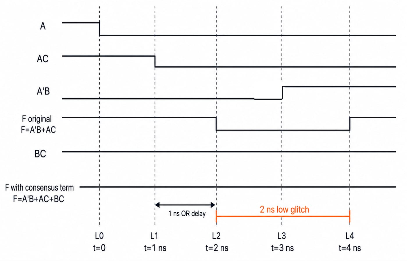
Consider F = A'B + AC with B=C=1 while A changes from 1 to 0. F should remain 1. With an AC path delay of 1 ns, an inverter-plus-AND delay of 3 ns for A'B, and an OR delay of 1 ns, AC falls at t=1 ns and F falls at t=2 ns. A'B rises at t=3 ns and F recovers at t=4 ns. The low glitch lasts 2 ns.
The consensus term BC remains 1 throughout. Adding it gives the equivalent, hazard-resistant form F = A'B + AC + BC.
Other traps come from careless reading or unstated assumptions:
Confusing active-low and active-high pins.
Using binary order instead of Gray-code adjacency on a K-map.
Treating XOR as OR or dropping a final carry-out.
Reversing MUX select-line order.
Assuming invalid decoder or BCD inputs are don't-cares without permission.
Ignoring path delay after simplifying the equation.
Practise deriving an output from a gate diagram, assigning MUX data inputs, combining decoder minterms, tracing carry and spotting a hazard. KnowledgeGate's Digital Electronics practice bank carries over 260 questions on combinational circuits alone. Use the GATE Test Series to apply these skills under exam-style timing.
The short version and what to practise next
Identify the present inputs, complete the truth table, write the canonical function, minimise it, choose a device, preserve polarity, verify representative rows, then check delay and hazards. The majority function, 4-bit addition, MUX assignment, decoder realisation and parity check are five forms of the same process.
Next, redraw the majority circuit and the 4:1 MUX example without looking. Change one input row and recompute the result. For a sequenced route through the wider subject, work through GATE Guidance by Sanchit Sir.
Keep learning

Functional Completeness in Digital Logic: NAND, NOR and Worked Examples
Learn what makes a Boolean operator set complete, how NAND and NOR recover a standard basis, and how to verify a four-gate NAND construction.
Updated 2 Oct 20266 min readDigital Logic
Boolean Function Counts: Formulas, Worked Examples and Exam Traps
Build the master Boolean-function formula from output choices, then learn how common restrictions change the count through combinations, pairing and inclusion-exclusion.
Updated 27 Sep 20266 min readDigital Logic

Analog-Digital Conversion Basics: ADC, DAC, Worked Examples and Exam Patterns
Build ADC and DAC basics from one consistent transfer model, then practise code selection, reconstruction error, flash and SAR conversion, and bit-depth calculations.
Updated 25 Sep 20266 min readDigital Logic

Universal Realization with NAND and NOR Gates: Concepts, Worked Example and Exam Patterns
Learn why NAND and NOR are universal, then implement one three-variable function using four NAND gates and four NOR gates with verified input traces.
Updated 23 Sep 20265 min readDigital Logic