The chip select logic for a certain DRAM chip in a memory system design is…
GATE · 2019 · CS · Computer Science & IT
The chip select logic for a certain DRAM chip in a memory system design is shown below. Assume that the memory system has 16 address lines denoted by A15 to A0. What is the range of addresses (in hexadecimal) of the memory system that can get enabled by the chip select (CS) signal?
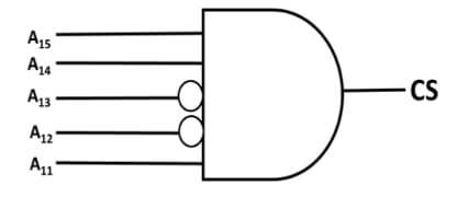
- A.
C800 to CFFF
- B.
CA00 to CAFF
- C.
C800 to C8FF
- D.
DA00 to DFFF
Attempted by 42 students.
Show answer
Correct answer: A
Explore the full course: Iocl Engineers Officers Grade A Paper 2
Loading lesson…