Memory Chip Configuration: Chip Count, Address Lines and Two Worked Designs
Learn to separate depth expansion from width expansion, wire chip banks, derive address pins and check hexadecimal ranges with two complete examples.
KnowledgeGate Team
Exam prep & CS education
Updated 25 Oct 20265 min read

A specification such as 8K x 16 using 2K x 8 chips mixes locations, word width, address pins and chip-select logic, so one memorised chip-count formula is not enough. Depth expansion chooses banks; width expansion puts chips in parallel. Computer Memory Basics: Addressability, Capacity and Chip Organisation with Worked Examples establishes addressability and capacity. Memory-chip configuration then separates bank wiring, chip-select decoding and hexadecimal placement from those foundation calculations. Memory-chip organisation differs from cache placement policies. For wider subject study, the GATE CS Exam Preparation Courses and Test Series covers the rest of the syllabus.
Memory chip configuration notation: what 2K x 8 means
A memory specification is number of addressable words x bits per word. In a 2K x 8 chip, 2K = 2 x 1024 = 2048 = 2^11 locations, and each location holds 8 bits. Its storage is 2048 x 8 = 16,384 bits = 16 Kibits = 2 KiB. It is 16 Kibits, not 16 KiB.
Specification | Locations | Word width | Address lines | Data lines | Total capacity |
|---|---|---|---|---|---|
| 2048 | 8 bits | 11 | 8 | 16 Kibits = 2 KiB |
| 8192 | 16 bits | 13 | 16 | 128 Kibits = 16 KiB |
Address pins depend on locations: address lines = log2(words). Data pins equal the word width. Total stored bits check capacity, not address-line count.
For the wider system context, Memory Hierarchy and Virtual Memory Explained shows where memory levels fit.
Memory chip configuration method: separate depth from width
Use this sequence for a chip-organisation problem:
Normalise
Kas2^10.Identify the target number of words and target bits per word.
Calculate
depth factor = target words / chip words.Calculate
width factor = target word width / chip word width.Calculate
total chips = depth factor x width factor.
These ratios assume exact integer expansion. Width expansion puts chips in parallel: they share address and control signals, are selected together, and carry different data-bit slices. Depth expansion creates banks. Banks may share the data bus, but a decoder enables only one for each address.
For an exact build, confirm total chip capacity = target capacity. Otherwise, choose the next usable organisation and leave some locations or data bits unused. A fractional chip count is never valid.
Worked memory-chip design: build 8K x 16 from 2K x 8 chips
For the depth:
depth factor = 8K / 2K = 4
The design needs four banks. For the width:
width factor = 16 / 8 = 2
Each bank needs two chips in parallel, so:
total chips = 4 x 2 = 8 chips
Capacity confirms it: the target stores 8192 x 16 = 131,072 bits, and the chips provide 8 x (2048 x 8) = 131,072 bits.
Organise the result as a 4 banks x 2 chips matrix. In each bank, the LOW chip supplies D7-D0 and the HIGH chip supplies D15-D8. Both are active together, so one address accesses one 16-bit word.
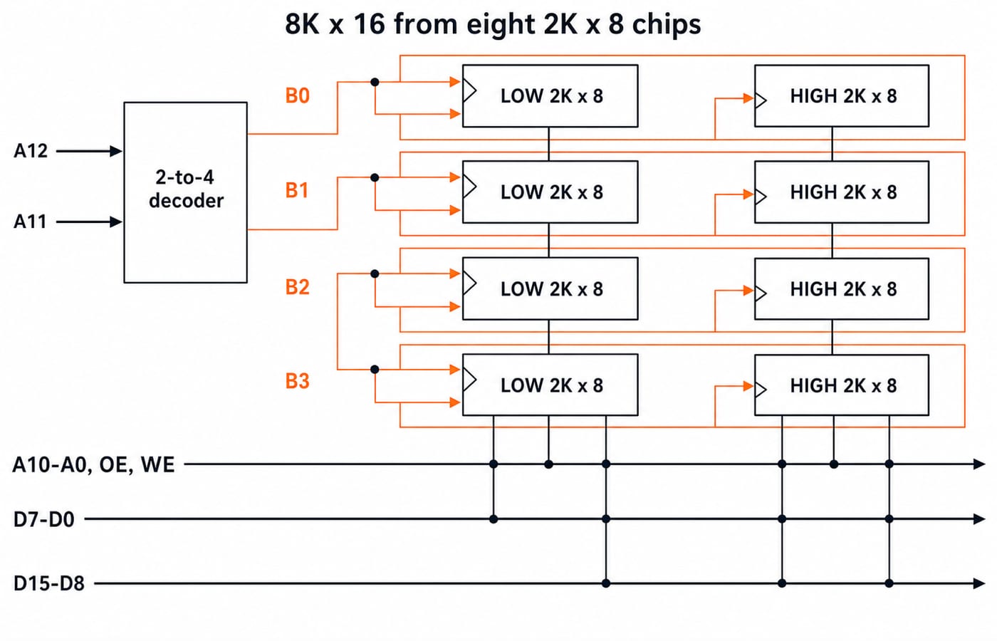
Address lines and chip-select decoding in the 8K x 16 design
The complete memory needs log2(8192) = 13 address lines, A12-A0. Each chip needs log2(2048) = 11, so connect A10-A0 to all eight chips.
The remaining address lines, A12-A11, feed a 2-to-4 decoder:
| Selected bank |
|---|---|
| B0 |
| B1 |
| B2 |
| B3 |
Each decoder output selects a two-chip bank, not one chip. The 16 data lines split across its LOW and HIGH chips, while the four banks cover different address ranges. Keep OE and WE generic because active levels depend on the device.
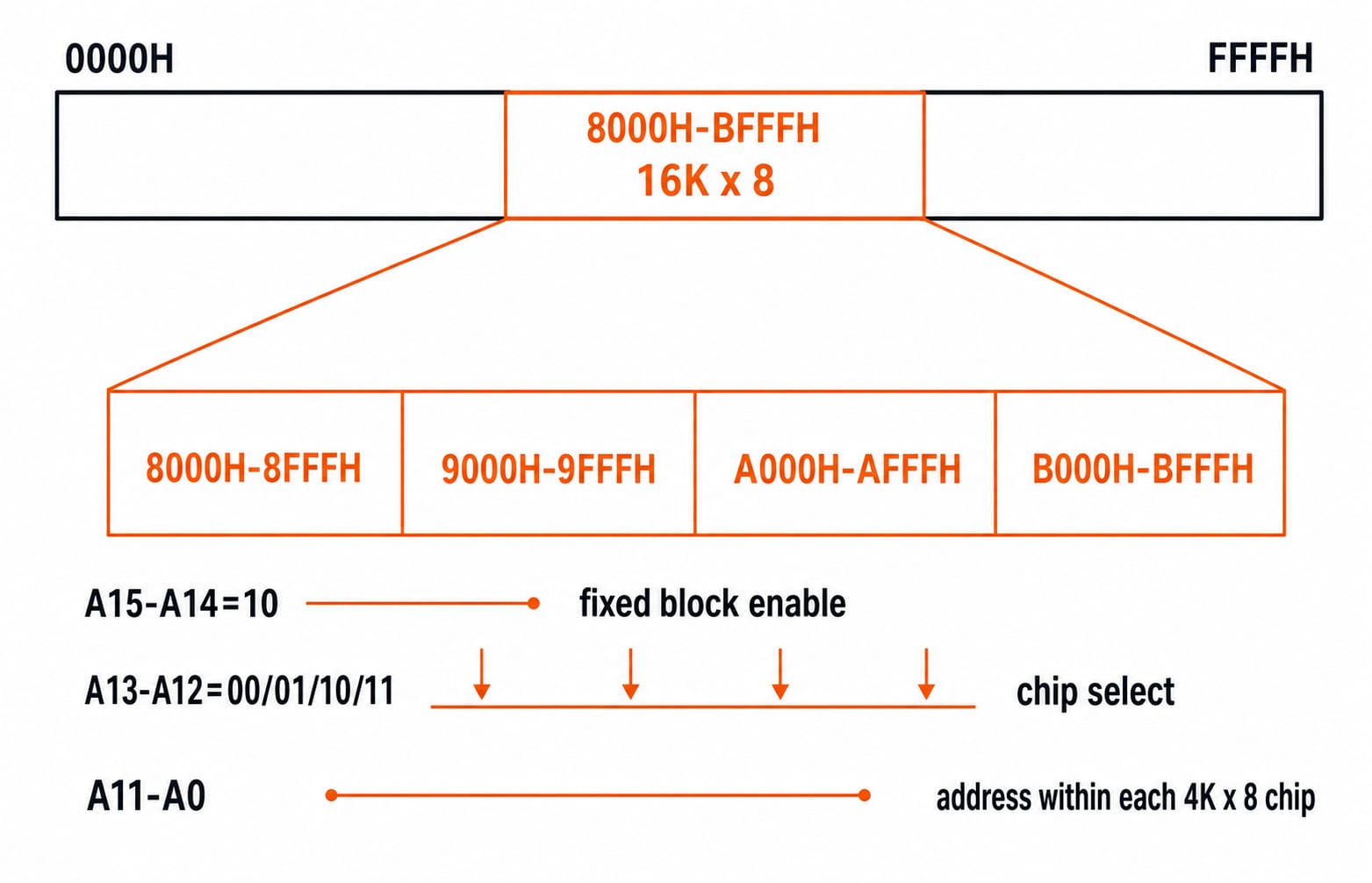
Worked address map: place 16K x 8 from 4K x 8 chips at 8000H
In a 16-bit, byte-addressed address space, place a 16K x 8 block at 8000H using 4K x 8 chips. The depth factor is 16K / 4K = 4, the width factor is 8 / 8 = 1, and the total is 4 x 1 = 4 chips. Each chip has 4K = 4096 = 2^12 locations, addressed by A11-A0.
The block size is 16K = 16,384 = 4000H. Both endpoints belong to it, so use the inclusive-end rule:
end = 8000H + 4000H - 1 = BFFFH
Chip | Address range | Range size |
|---|---|---|
Chip 0 |
|
|
Chip 1 |
|
|
Chip 2 |
|
|
Chip 3 |
|
|
Across 8000H-BFFFH, A15-A14 = 10 identifies the block. A13-A12 = 00, 01, 10, 11 selects Chips 0 to 3, and A11-A0 selects one of 4096 locations inside that chip.
Memory chip configuration traps and corrections
Trap | Wrong result | Correction |
|---|---|---|
Treating | 16 KiB | It is 16 Kibits, which equals 2 KiB |
Using | 14 address lines | Use |
Adding depth and width factors |
| Multiply them: |
Decoding eight individual chips | Eight independent selects | Decode four banks, each containing two parallel chips |
Treating |
| Subtract 1 for an inclusive range: |
Before calculating, read 8K x 16 aloud as “8192 words, 16 bits in each word”. This verbal unit check catches most bits-versus-words errors.
There is also an important non-integer edge case. A 12-bit target word built from 8-bit chips needs two chips in parallel. They provide 16 physical data bits, with four unused. The answer cannot be 12 / 8 = 1.5 chips.
How exams test memory chip configuration
Questions take four common shapes: forward design, reverse inference from pins, bus and decoder wiring, and hexadecimal range mapping. For example, a chip with 12 address pins and 8 data pins is:
2^12 x 8 = 4096 x 8 = 4K x 8 = 32 Kibits = 4 KiB
Use this 30-second verification checklist:
Address lines equal
log2(words).All width chips in the selected bank are active.
Only one depth bank is active.
Capacities match for an exact build.
Inclusive range size equals
end - start + 1.
Chip-bank selection and cache mapping are different operations. Continue with Cache Memory: Mapping and Hit Ratio for the cache concept.
These design calculations are fixed computer-organisation results, so the same method carries across chip-count, decoder-wiring and address-range questions. Work through a few of each shape until the steps come without notes.
Memory chip configuration: the short version and next step
Expand width with parallel chips, expand depth with decoded banks, multiply the two factors, then verify capacity and address pins. The main result is 8K x 16 from 2K x 8 = 4 depth banks x 2 width chips = 8 chips.
Words determine address lines, bits per word determine width wiring, and the unused high address lines select the bank. After you can reproduce both designs without notes, the GATE Test Series: Mocks and Topic-wise Tests is an optional next step for structured practice.
Keep learning

Pipelining Basics in Computer Architecture: Clock Cycle, Speedup and Hazard Worked Examples
Learn how to calculate a pipeline clock, fill and drain time, finite-batch speedup, latency, throughput, and the cost of a load-use stall.
Updated 23 Oct 20266 min readComputer Organization & Architecture

Data Manipulation Micro-Operations in COA: Arithmetic, Logic and Shift Operations Worked Step by Step
Learn a fixed-width method for tracing arithmetic, logic, and shift micro-operations. Every example tracks register values, result bits, carry, and overflow.
Updated 19 Oct 20265 min readComputer Organization & Architecture
Assembly Language and Assembler Design: Two-Pass Translation with a Complete Worked Example
Follow a 16-bit Basic Computer program through pass one, pass two, hexadecimal encoding and execution, with every symbol, address and result shown.
Updated 15 Oct 20266 min readComputer Organization & Architecture

Computer Classification and Flynn’s Taxonomy: The Four Classes with a Worked Vector Example
A machine can belong to several computer classes at once. Learn the four classification axes, Flynn’s matrix, vector and multicore traces, and exam traps.
Updated 11 Oct 20266 min readComputer Organization & Architecture