Interface & Addressing MCQs: 12 Solved Questions with Explanations
Attempt 12 published interface and addressing questions, then use the explanations to connect device control, address mapping, protection and bus-rate calculations.
KnowledgeGate Team
Exam prep & CS education
Updated 30 Aug 20267 min read
Interface and addressing questions shift quickly from device registers and control signals to address-space partitioning and bus throughput. A reliable solution starts by identifying the interface mechanism, then writing the address or transfer-rate relation before inspecting the options. Attempt all 12 before reading the explanations, and classify each miss with the error-log table at the end. For broader preparation, use the GATE CS exam preparation courses and test series.
1. Interface units, wait states and handshaking
CPU and peripherals differ in speed, timing and signal format. Interfaces bridge them with registers, buffering and control. Separate waiting from acknowledging a transfer.
Q1. Why a CPU needs an interface unit
Which component of the computer is used to resolve the difference between CPU and the peripheral device?
(a) Memory unit
(b) Arithmetic Logic Unit
(c) Interface unit
(d) Control unit
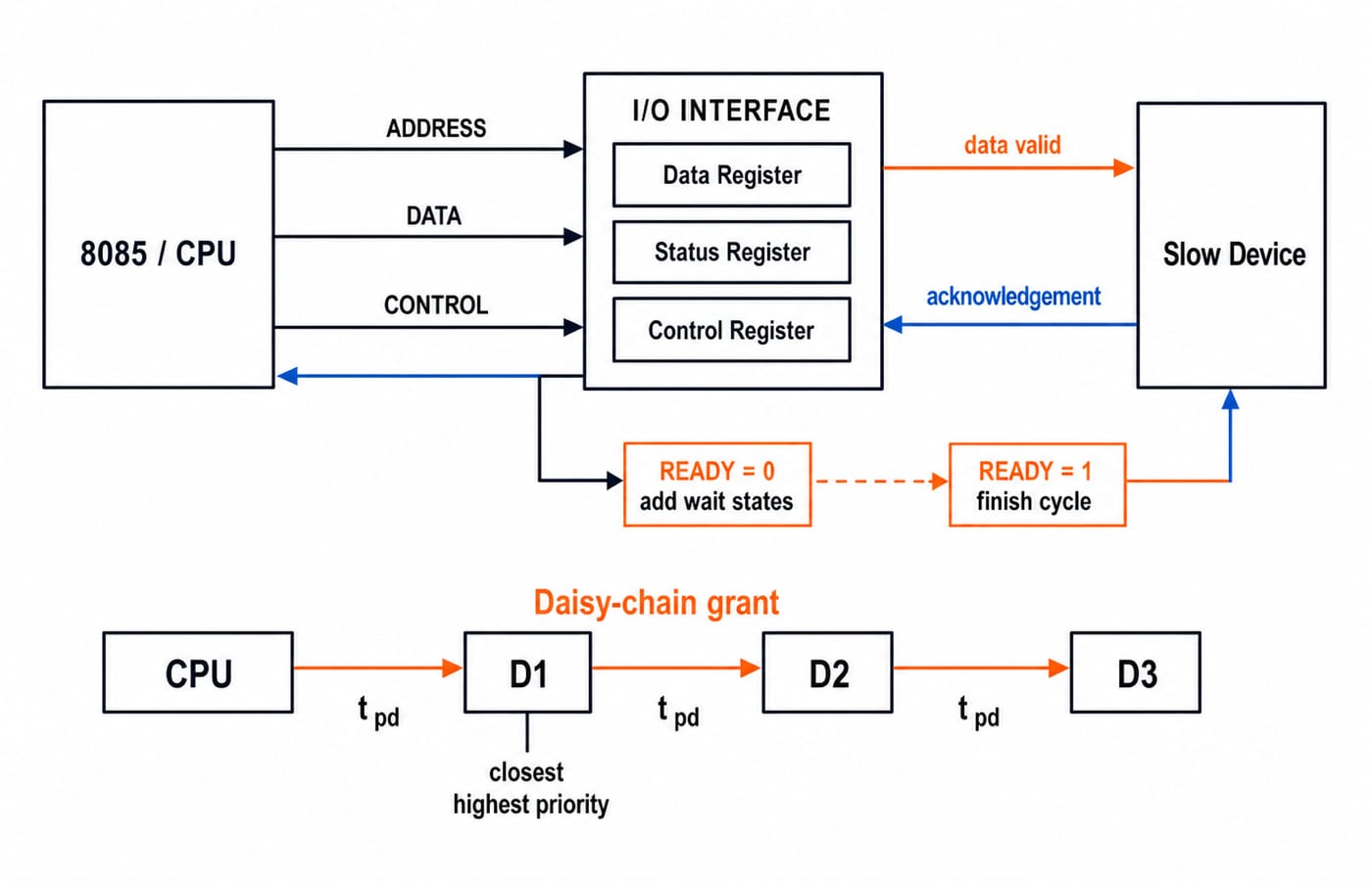
Answer: (c) Interface unit. Buffering and control bridge rate, timing and signal-format differences. Memory stores, the ALU computes, and the control unit coordinates, but none provides this device-facing bridge. DSSSB 2021. See the solved page.
Q2. Connecting slow memory to the 8085
A slow memory can be connected to 8085 by using
(a) INTR
(b)
(c) HOLD
(d) READY
Answer: (d) READY. When READY = 0, the 8085 inserts wait states and does not complete the bus cycle until the slow memory raises READY. INTR requests an interrupt, RESET IN resets the processor, and HOLD requests the bus for DMA. GATE 2001. See the solved page.
Q3. Acknowledging receipt of data
A unit receiving a data item sends back another control signal to acknowledge receipt of that data. This type of agreement between two independent units is known as ______.
(a) strobe control
(b) multitasking
(c) handshaking
(d) piggybacking
Answer: (c) handshaking. The sender marks data as available, and the receiver acknowledges acceptance. A strobe need not return an acknowledgement; piggybacking is a networking optimisation. Kendriya Vidyalaya Sangathan 2017. See the solved page.
2. Bus arbitration and coordination delay
Priority policy says who wins the bus. Physical timing says how long coordination signals travel.
Q4. Priority in a daisy chain
Which bus arbitration technique gives the highest priority to the device closest to the processor ?
(a) Daisy chaining
(b) Polling
(c) Independent requesting
(d) Time slice method
Answer: (a) Daisy chaining. The serial grant reaches the first device first. Wiring is simple, but position fixes priority, so a nearer requester can delay others. TPSC 2026. See the solved page.
Q5. What sets bus-coordination time
Which of the following determines the time it takes for devices to coordinate the use of the bus?
(a) Propagation delay
(b) Clock delay
(c) Cycle delay
(d) Data transfer delay
Answer: (a) Propagation delay. Request, grant and acknowledgement signals must reach the devices. Data-transfer delay concerns the later payload movement. DSSSB 2018. See the solved page.
3. Memory-mapped I/O, isolated I/O and programmed input
Memory-mapped I/O puts device registers in memory space for ordinary load and store access. Isolated I/O keeps separate port addresses and normally uses distinct I/O operations. Programmed input polls interface registers in dependency order.
Q6. Shared control lines versus a separate address space
State whether the following sentences are true or false.
(i) With memory-mapped I/O, a single read line and a single write line are needed on the bus.
(ii) With isolated I/O, the address space for I/O is isolated from that for memory.
(a) (i) – True, (ii) – True
(b) (i) – False, (ii) – False
(c) (i) – False, (ii) – True
(d) (i) – True, (ii) – False
Answer: (a) (i) – True, (ii) – True. Memory mapping reuses memory's read and write controls; isolated I/O separates port and memory addresses. Separate spaces do not imply identical controls. Navodaya Vidyalaya Samiti 2019. See the solved page.
Q7. What best characterises memory-mapped I/O
Of the following, which best characterizes computers that use memory-mapped I/O?
(a) The computer provides special instructions for manipulating I/O ports
(b) I/O ports are placed at addresses on the bus and are accessed just like other memory locations
(c) To perform I/O operations, it is sufficient to place the data in an address register and call channel to perform the operation
(d) I/O can be performed only when memory management hardware is turned on
Answer: (b). Ordinary addresses let memory-access instructions reach device registers. Option (a) fits isolated I/O; (c) and (d) do not define memory mapping. Indian Space Research Organization 2018. See the solved page.
Q8. Correct programmed-input sequence
The right sequence of CPU program to input data will be:
A. Read status register
B. Check flag bit
C. Read Data Register
D. Transfer data to memory
Choose the correct answer from the options given below:
(a) A, B, C, D
(b) B, A, C, D
(c) C, B, A, D
(d) A, C, B, D
Answer: (a) A, B, C, D. Read status, test the ready flag, read data, then store it. Another order breaks a dependency. UGC NET 2025. See the solved page.
4. Protecting memory-mapped device registers
No special I/O opcode does not mean no protection. The OS can restrict device-register pages through mappings and permissions.
Q9. I/O protection without explicit I/O instructions
Normally user programs are prevented from handling I/O directly by I/O instructions in them. For CPUs having explicit I/O instructions, such I/O protection is ensured by having the I/O instructions privileged. In a CPU with memory mapped I/O, there is no explicit I/O instruction. Which one of the following is true for a CPU with memory mapped I/O?
(a) I/O protection is ensured by operating system routine (s)
(b) I/O protection is ensured by a hardware trap
(c) I/O protection is ensured during system configuration
(d) I/O protection is not possible
Answer: (a) I/O protection is ensured by operating system routine (s). The OS controls device-register mappings, and hardware enforces their permissions. Illegal access may trap, but the trap is the outcome. Review Memory Management in OS: Paging and Segmentation for the page-permission model only. GATE 2005. See the solved page.
5. Address-bit calculations for memory-mapped I/O
Write the three leading bits separately from the other 29. This reveals both answers before you inspect the options.
Q10. Bits available for addressing
Consider a 32-bit hypothetical processor which supports 512 MWord memory. Processor uses the memory mapped IO configuration in which when 3 MSB bits of address is 1 assign them to IO ports. How many bits can be used for addressing?
(a) 23-bits
(b) 27-bits
(c) 29-bits
(d) None
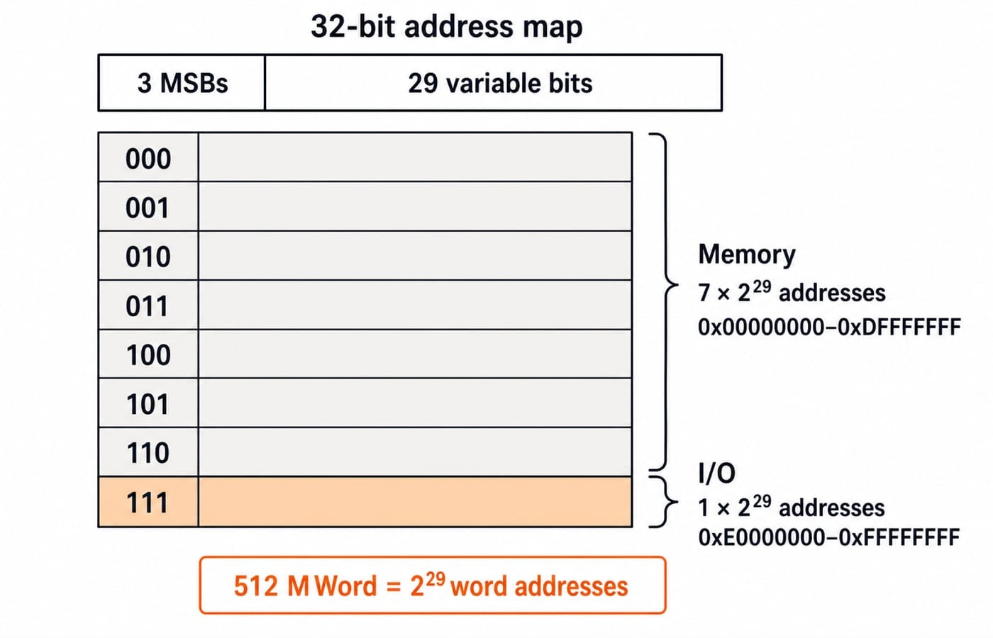
Answer: (c) 29-bits. Fixing three MSBs leaves 32 - 3 = 29 variable bits. Cross-check: 512 MWord = 512 x 2^20 = 2^9 x 2^20 = 2^29 word addresses. Reinforce the partition rule in the Interface & Addressing module.
Q11. Partitioning a 32-bit address space
A computer system that used memory mapped IO configuration, has a 32-bit address space. Address with 1’s in the three MSB refer to devices. What is the maximum amount of memory address and I/O port address that can be referenced in such a system respectively?
(a) and
(b) and
(c) and
(d) and
Answer: (c) and . Three MSBs make 2^3 = 8 regions of 2^29 addresses. 111 gives I/O from 0xE0000000 to 0xFFFFFFFF; 000 to 110 give memory from 0x00000000 to 0xDFFFFFFF. Check: 7 x 2^29 + 1 x 2^29 = 2^32. The partition accounts for all addresses, so the memory and I/O totals add back to the full 32-bit space.
6. Bus-cycle throughput with actual units
Calculate cycles per second, then bytes per cycle. Do not use 8 MHz directly or treat 16 bits as 16 bytes.
Q12. Maximum data-transfer rate
Consider a 32-bit microprocessor, with a 16-bit external data bus, driven by an 8 MHz input clock. Assume that this microprocessor has a bus cycle whose minimum duration equals four input clock cycles. What is the maximum data transfer rate for this microprocessor ?
(a) bytes/sec
(b) bytes/sec
(c) bytes/sec
(d) bytes/sec
Answer: (b) bytes/sec. Bus cycles per second = 8 MHz / 4 = 2 x 10^6. Bytes per cycle = 16 / 8 = 2. Rate = 2 x 10^6 x 2 = 4 x 10^6 bytes/sec. UGC NET 2015. See the solved page.
7. Error log and next practice step
Question family | First line to write | Common trap | Self-check |
|---|---|---|---|
Interface role | Bridge differences | CPU internals | Device-facing |
READY/wait state |
| HOLD | Q2 needs READY |
Handshaking | Data, then ACK | Strobe | Return signal |
Daisy priority | Serial grant | Position | D1 is closest |
Mapped/isolated | Address spaces | Control lines | Two models |
Polling | Status first | Early data |
|
Protection | OS mappings | Impossible | Access can trap |
Address partition |
| 30-bit regions |
|
Bus throughput | Cycles, bytes | 16 bytes | Use 2 bytes |
Redo Q6, Q8, Q11 and Q12 without notes. Try Floating Point Representation: IEEE 754 Format next and Sequential Circuits: Flip-Flops and Counters for hardware foundations. Study with GATE Guidance by Sanchit Sir, then take timed mixed-topic practice in the GATE Test Series.
Keep learning
Data Manipulation Micro-Operations MCQs: 10 Solved Questions with Explanations
Solve 10 micro-operations MCQs with step-by-step explanations of shifts, ALU behaviour, register logic, Booth recoding and control width.
Updated 20 Oct 20267 min readComputer Organization MCQs
Performance & Speedup MCQs: 12 Solved Pipelining Questions
Work through 12 solved pipelining questions step by step, from finite pipeline time and latch overhead to bubbles, MIPS, CPI and bottleneck splitting.
Updated 16 Oct 20268 min readComputer Organization MCQs
Multiprocessor Classification MCQs: 8 Solved MCQs and 2 Concept Checks
Work through the complete mapped pool: eight objective items plus two optionless concept checks. Explanations cover Flynn's taxonomy, coupling, bus facts, and parallel efficiency.
12 Oct 20267 min readComputer Organization MCQs
Input Output Organisation MCQs: 12 Cross-Concept COA Questions Solved
Test 12 Input Output Organisation MCQs across storage, spooling, I/O instructions, interrupts, DMA, arbitration and bus bandwidth.
8 Oct 20268 min readComputer Organization MCQs