What does the circuit shown below represent?
2017
What does the circuit shown below represent?
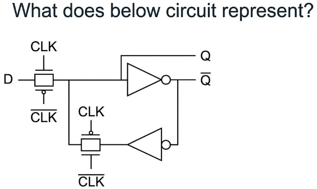
Answer: B. Positive level sensitive D-latch — Concept. A CMOS transmission gate conducts when its plain (n-channel) control is 1 while its bubbled (p-channel) control is 0. A clocked storage cell is…
- A.
D flip-flop
- B.
Positive level sensitive D-latch
- C.
Negative level sensitive D-latch
- D.
None of the above
Attempted by 28 students.
Show answer & explanation
Correct answer: B
Concept. A CMOS transmission gate conducts when its plain (n-channel) control is 1 while its bubbled (p-channel) control is 0. A clocked storage cell is level-sensitive — a latch — when one clocked switch sits in the input path and a second, oppositely clocked switch closes an inverter feedback loop: that arrangement gives exactly one transparent window per clock period, and during it the output tracks the input continuously. The same cell is edge-triggered — a flip-flop — only when two such stages are cascaded on opposite clock phases, so data advances one stage per half-period and can reach the output only through the handover at a clock transition.
Application. Read the two transmission gates of the figure by their control labels:
Input gate: plain control = CLK, bubbled control = CLK-bar, so it conducts while CLK = 1 and passes D to the internal node.
That internal node is brought out as Q, and the inverter it drives produces Q-bar.
Feedback gate: bubbled control = CLK, plain control = CLK-bar, so it conducts while CLK = 0 and returns the second inverter output to the same internal node.
While CLK = 1 the input gate conducts and the feedback gate is open, so the cell is transparent and Q = D.
While CLK = 0 the input gate is open and the feedback gate conducts, so the two inverters form a cross-coupled loop that holds the value present at the falling edge.
Cross-check. Test the structure against the alternatives:
Only one clocked stage lies between D and Q, so there is no master-slave handover: the output changes throughout the high phase, not only at an edge. That rules out edge-triggered operation.
The transparent window coincides with CLK = 1 and the hold window with CLK = 0, so the level sensitivity is positive, not negative.
A standard named structure does describe the cell, so the list of named structures is not exhausted.
Result. The circuit is a positive level-sensitive D-latch: transparent (Q = D) while CLK is high, and holding the stored value while CLK is low.