The figure above shows two transistor-level static CMOS circuits, labelled A…
2017
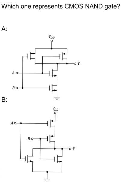
The figure above shows two transistor-level static CMOS circuits, labelled A and B. Which one represents a CMOS NAND gate?
Answer: A. Figure A — Concept: a static CMOS gate is built from two complementary switch networks. A pull-up network (PUN) of p-channel MOSFETs sits between VDD and the output…
- A.
Figure A
- B.
Figure B
- C.
Both A and B
- D.
None of the above
Attempted by 5 students.
Show answer & explanation
Correct answer: A
Concept: a static CMOS gate is built from two complementary switch networks. A pull-up network (PUN) of p-channel MOSFETs sits between VDD and the output node, and a pull-down network (PDN) of n-channel MOSFETs sits between the output node and ground. A PMOS conducts when its gate is LOW and an NMOS conducts when its gate is HIGH; transistors wired in series conduct only when every one of them is on, while transistors wired in parallel conduct when any one of them is on. The two networks are duals of each other, so wherever the pull-down network is a series chain the pull-up network is a parallel pair, and vice versa.
This makes the series/parallel pattern the fingerprint of the logic function realised:
Function | Output goes LOW when | Pull-down network (NMOS) | Pull-up network (PMOS) |
|---|---|---|---|
NAND, Y = (A · B)′ | both inputs are HIGH | two devices in series | two devices in parallel |
NOR, Y = (A + B)′ | either input is HIGH | two devices in parallel | two devices in series |
Application: read the two networks of each drawn circuit and match them against that pattern.
In the circuit labelled A the two n-channel transistors are stacked one above the other, forming a single path from the output node down to ground, so its pull-down network is a series chain. Its two p-channel transistors both sit between VDD and the output node, so its pull-up network is a parallel pair. A series pull-down with a parallel pull-up is the NAND pattern, so the circuit labelled A is the CMOS NAND gate.
In the circuit labelled B the two p-channel transistors are stacked from VDD down to the output node, so its pull-up network is a series chain, and its two n-channel transistors both sit between the output node and ground, so its pull-down network is a parallel pair. A series pull-up with a parallel pull-down is the NOR pattern, so the circuit labelled B is a CMOS NOR gate.
The two drawn circuits therefore realise different logic functions, so they cannot both be the NAND gate; and because the circuit labelled A is the NAND gate, the answer is not "none of the above" either.
Cross-check: evaluate the circuit labelled A input combination by input combination. Input A drives the upper n-channel device and one p-channel device; input B drives the lower n-channel device and the other p-channel device.
A | B | Series NMOS chain | Parallel PMOS pair | Y |
|---|---|---|---|---|
0 | 0 | open | conducting | 1 |
0 | 1 | open | conducting | 1 |
1 | 0 | open | conducting | 1 |
1 | 1 | conducting | open | 0 |
The output is LOW for A = B = 1 and HIGH for every other input combination, which is exactly Y = (A · B)′. The circuit labelled A is therefore the CMOS NAND gate.