The following figure is a representation of which logic gate?
2017
The following figure is a representation of which logic gate?
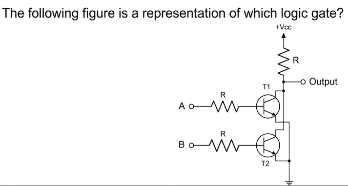
Answer: D. 2 input NOR Gate — Concept: In resistor–transistor logic (RTL) each input drives the base of an NPN transistor through a series resistor. A transistor whose base is HIGH…
- A.
2 input AND Gate
- B.
2 input OR Gate
- C.
2 input NAND Gate
- D.
2 input NOR Gate
Attempted by 4 students.
Show answer & explanation
Correct answer: D
Concept: In resistor–transistor logic (RTL) each input drives the base of an NPN transistor through a series resistor. A transistor whose base is HIGH saturates and behaves as a closed switch between its collector and its emitter, while a transistor whose base is LOW stays cut off and behaves as an open switch. One pull-up resistor from +Vcc holds the common collector node HIGH only while no transistor conducts.
How those switches share that node is what fixes the logic function: transistors wired in parallel — every collector on the output node and every emitter on ground — drag the output LOW as soon as any one of them conducts, whereas transistors stacked in series between the output node and ground drag it LOW only when all of them conduct.
Application: Here T1 takes input A and T2 takes input B, each through its own base resistor R. Both collectors sit on the same node that the pull-up resistor R feeds and that Output taps, and both emitters return to ground, so the two transistors stand in parallel. Testing all four input combinations:
A = 0, B = 0 — both transistors are cut off, so no path runs from the output node to ground and the pull-up resistor lifts the node to +Vcc; Output = 1.
A = 1, B = 0 — T1 saturates and clamps the output node to ground; Output = 0.
A = 0, B = 1 — T2 saturates and clamps the output node to ground; Output = 0.
A = 1, B = 1 — both transistors saturate and hold the output node at ground; Output = 0.
Output is HIGH for exactly one combination, A = B = 0, which is the truth table of Y = (A + B)′ — a 2-input NOR gate.
Cross-check against the other gate functions:
Y = A·B would need Output HIGH only at A = B = 1, but that combination drives the node to ground here.
Y = A + B would need Output LOW only at A = B = 0, but that is the single combination leaving Output HIGH here.
Y = (A·B)′ requires both transistors to conduct before the output falls, which is the series (stacked) arrangement, not the parallel one drawn.
Y = (A + B)′ reproduces the derived table exactly, so the figure is a 2-input NOR gate.