Memory Interfacing for GATE: Chip-Count and Address-Decoding Numericals, Fully Worked
Separate words from bits, split the address correctly, and verify the result with a gap-free hexadecimal map. This guide works through depth and width expansion step by step.
KnowledgeGate Team
Exam prep & CS education
Updated 24 Sep 20265 min read55 views
Memory-interfacing questions look like circuit design, but most of them are three divisions followed by one decoder. The usual mistake is mixing bits with words or sending the wrong address lines to the decoder. Keep those quantities separate, and the circuit becomes a clean numerical.
What the question is really asking: three quantities
A memory-interfacing problem normally asks for one or more of these:
the number of memory chips required
the number of address lines required
the size of the chip-select decoder
Start by reading the chip notation correctly. A 2K x 8 chip has 2K words, with 8 bits in each word. Since 1K means 2^10, the chip has 2 x 1024 = 2048 addressable words. Its total capacity is 2048 x 8 = 16,384 bits, but its depth is still 2048 words.
That distinction matters because address lines select words, not individual stored bits, unless the question explicitly describes bit-addressable memory. Keep two columns on rough paper: word count and bits per word. Never add them, and do not replace 1024 with 1000. Similarly, 1M means 2^20.
The two-part address: in-chip lines versus chip-select lines
If a memory contains N addressable words, it needs log2(N) address lines. If each chip contains M words, the lowest log2(M) lines choose a word inside every chip. The remaining high-order lines decide which chip is active.
Suppose the full memory needs t address lines and one chip needs m. Then:
in-chip address lines = m
chip-select lines = t - m
decoder size = (t - m)-to-2^(t - m)
Depth expansion adds more words, so it adds high-order selection lines and banks. Width expansion makes each word wider, so chips sit side by side. Those chips share the same address and chip-select signals. Width expansion does not create extra address lines.
Example: build 16K x 8 from 2K x 8 chips
The target is 16K x 8, and one available chip is 2K x 8.
Step 1: Find the depth factor.
Required chips for depth = 16K / 2K = 8.
The target width and chip width are both 8 bits, so the width factor is 8 / 8 = 1. Total chips = 8 x 1 = 8.
Step 2: Find the total address lines.
16K words = 16 x 1024 = 16,384 = 2^14 words. Therefore, the complete memory needs 14 address lines, A0 through A13.
Step 3: Find the lines used inside a chip.
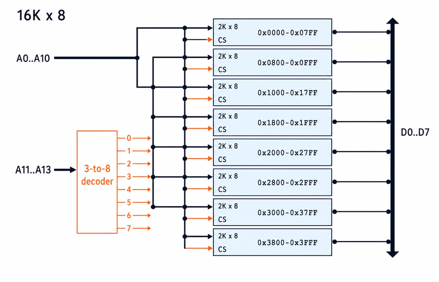
Each chip stores 2K = 2048 = 2^11 words. It therefore needs 11 lines, A0 through A10. Wire these lines to all eight chips in parallel.
Step 4: Design chip selection.
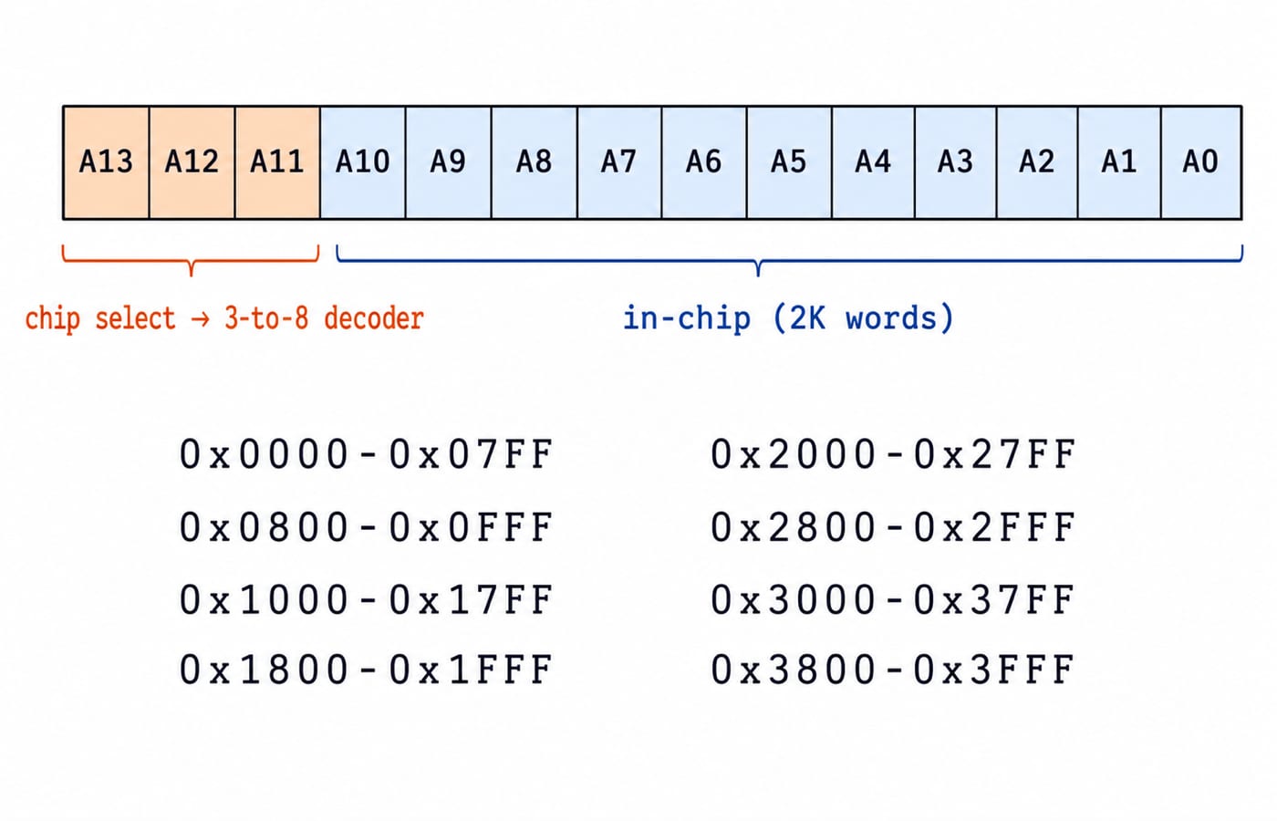
High-order lines = 14 - 11 = 3. Feed A11, A12 and A13 to a 3-to-8 decoder. Exactly one of its eight outputs enables one chip.
Step 5: Verify with the address map.
One chip spans 2K addresses, which is 0x800 addresses. The inclusive ranges are:
Chip | Start address | End address |
|---|---|---|
0 | 0x0000 | 0x07FF |
1 | 0x0800 | 0x0FFF |
2 | 0x1000 | 0x17FF |
3 | 0x1800 | 0x1FFF |
4 | 0x2000 | 0x27FF |
5 | 0x2800 | 0x2FFF |
6 | 0x3000 | 0x37FF |
7 | 0x3800 | 0x3FFF |
The union is 0x0000 to 0x3FFF. Its size is 0x3FFF - 0x0000 + 1 = 0x4000 = 16,384 addresses = 16K. The +1 is essential because both endpoints are included. This gap-free map independently confirms the chip count and decoder.
Width expansion and the combined case
For pure width expansion, build 4K x 16 from 4K x 8 chips. The depths already match. The width factor is 16 / 8 = 2, so place two chips side by side. Both receive the same 12 address lines because 4K = 2^12, and both are enabled together. One supplies eight data bits and the other supplies the remaining eight. No bank-selection decoder is needed.
Now build 8K x 16 from 2K x 8 chips. Compute the factors separately:
depth factor = 8K / 2K = 4 banks
width factor = 16 / 8 = 2 chips per bank
total chips = 4 x 2 = 8
The target has log2(8K) = 13 address lines. Each chip uses log2(2K) = 11 in-chip lines. The remainder is 13 - 11 = 2, so a 2-to-4 decoder selects one of four banks. Each decoder output enables both chips in its bank at the same time.
The general formula is:
chips = (target words / chip words) x (target word bits / chip word bits)
Use it only after checking that each ratio is an integer, as standard exam problems normally choose compatible sizes.
The traps GATE plants here
The first trap is using all address lines as decoder inputs. Only the unused high-order remainder selects a chip or bank. The second is treating data-bus width as address depth. Doubling a word from 8 to 16 bits doubles chips across the bank, not address lines.
Capacity units are another favourite. If a chip is given as 16 Kbit and the memory is organised in 8-bit words, first convert its depth: 16 Kbit / 8 bits per word = 2K words. Only then calculate address lines.
Finally, complete decoding gives every physical word one address. Incomplete decoding ignores one or more high-order lines, so the same chip responds at multiple addresses. That creates aliases, not extra storage.
How GATE tests memory interfacing
Typical questions ask for chip count, decoder size, address-line count or the exact range assigned to a chip. A reverse question may give the decoder and total address bus, then ask for the chip depth. Work backward using the same split.
Check the current syllabus and any weightage details on the official GATE 2027 exam-papers and syllabus page from IIT Madras. The numerical method itself stays fixed. For adjacent address-translation ideas, Memory Hierarchy and Virtual Memory: paging, the TLB, and address translation makes a useful follow-on, while Cache memory: mapping techniques and hit ratio, with the exam angle carries the same discipline into cache fields.
Memory interfacing: the four-line exam checklist
Use the words ratio for depth, the bits ratio for width, and multiply them for the total chip count. Low-order lines address a word inside a chip. The remaining high-order lines select a bank. Finish by drawing a hexadecimal map and checking its inclusive size.
Now drill mixed chip-count and decoding questions in the GATE Test Series, and use GATE Guidance by Sanchit Sir for structured coverage. The GATE CS preparation catalogue gives you the wider route through the subject.
Keep learning
ISRO Scientist/Engineer CS Syllabus vs GATE CS: The Subject Overlap Map
See which core CS subjects transfer directly from GATE to ISRO, what drops out, how the question texture changes and where an ISRO-specific polish helps.
Updated 5 Oct 20264 min readGATE Strategy & Roadmap

Union-Find for GATE: Union by Rank, Path Compression and the Near-Constant Bound
Trace seven unions, inspect the final ranks, then compress the deepest path by hand. The worked forest makes the inverse-Ackermann bound much less mysterious.
Updated 1 Oct 20265 min readGATE Strategy & Roadmap
RAID Levels for GATE: Striping, Mirroring, Parity and the Two Capacity Formulas
Stop memorising RAID names in isolation. Tie each level to usable capacity, failure tolerance and write cost, then test the formulas on one eight-disk array.
Updated 26 Sep 20265 min read58 viewsGATE Strategy & Roadmap
KMP and Rabin-Karp for GATE: The Failure Function and Rolling Hash, Fully Solved
Build the LPS array without guessing, trace a KMP fallback that never moves the text index back, and calculate every Rabin-Karp window hash by hand.
Updated 23 Sep 20266 min readGATE Strategy & Roadmap