The following figure represents which kind of flip-flop?
2017
The following figure represents which kind of flip-flop?
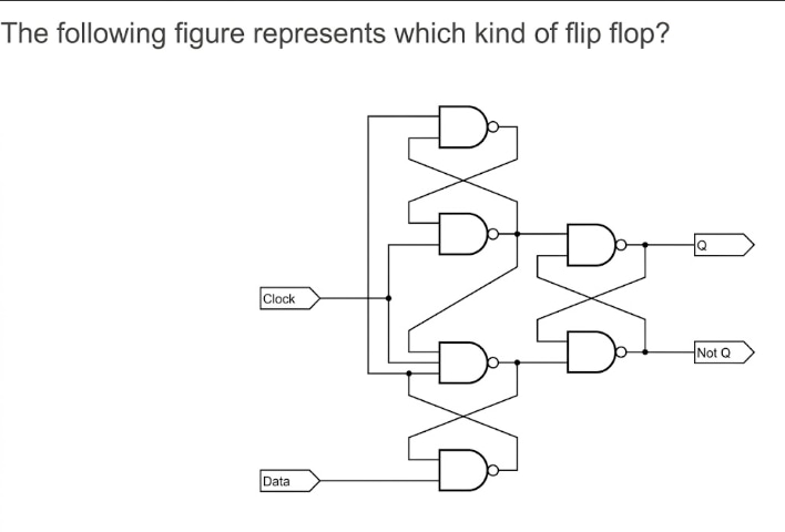
Answer: C. Positive Edge Triggered D Flip-flop — Concept. A flip-flop is classified along two independent axes. The first is its data terminal: a D-type element has one data input whose value is transferred…
- A.
T Flip-flop
- B.
D Flip-flop
- C.
Positive Edge Triggered D Flip-flop
- D.
Negative Edge Triggered D Flip-flop
Attempted by 26 students.
Show answer & explanation
Correct answer: C
Concept. A flip-flop is classified along two independent axes. The first is its data terminal: a D-type element has one data input whose value is transferred to the output, while a T-type element has a toggle input that either holds or complements the stored bit. The second is when the element samples that input: a level-triggered latch follows its input throughout the interval the clock is asserted, whereas an edge-triggered flip-flop samples only during a clock transition — the rising 0 to 1 transition for positive-edge triggering, the falling 1 to 0 transition for negative-edge triggering. At gate level, edge triggering is produced by a steering network inserted between the data input and the output latch, and the active edge is fixed by whether the clock reaches that steering network directly or through an inversion.
Application. Reading the given figure gate by gate:
The circuit has exactly two external inputs, Clock and Data, and two outputs, Q and Not Q. One data terminal named Data identifies a D-type element; there is no toggle terminal.
The two right-hand NAND gates are cross-coupled with each other and drive Q and Not Q. That pair is a NAND SR latch — the memory element that actually stores the bit.
The two middle NAND gates drive the set and reset inputs of that latch, and the Clock line fans out directly to both of them. They are therefore the steering gates that decide when the latch is allowed to change.
The top and bottom NAND gates, cross-coupled with the middle pair, hold the sampled value of the data input. Data enters the network at the bottom gate only.
While Clock = 0, both steering NAND gates are forced to output 1. For a NAND SR latch the input pair (1, 1) is the hold condition, so Q cannot change at any moment the clock is low, however the data input moves.
At the instant Clock rises from 0 to 1, whichever steering gate has its other input at 1 drops its output to 0 and delivers a single set or reset pulse, determined by the value of the data input immediately before that transition. The feedback around the input gates then locks the steering outputs, so later changes of the data input while Clock stays at 1 have no effect.
The stored bit can therefore change only during the 0 to 1 transition of the clock: the element is edge-triggered, and its active edge is the rising one.
Cross-check. The schematic contains no inverter and no bubble on the Clock terminal, so the clock reaches the steering gates uninverted. The falling-edge design is the same six-NAND network with the clock inverted before it fans out, which is drawn as an inverter or a bubble at the Clock input; its absence here settles the edge. A merely level-triggered D latch is a different circuit again — four gates, with the clock gating the data input straight into the SR latch. The two extra gates and their feedback paths seen here are precisely what converts level control into edge control.
Element | Data terminal | When the stored bit can change |
|---|---|---|
T flip-flop | T (toggle) | On the active clock edge: holds when T = 0, complements when T = 1 |
D flip-flop (generic name) | D (data) | Not fixed by the name: neither the triggering mechanism nor the active edge is stated |
Positive-edge-triggered D flip-flop | D (data) | Only at the 0 to 1 transition of the clock |
Negative-edge-triggered D flip-flop | D (data) | Only at the 1 to 0 transition of the clock |
Result. The figure is the standard six-NAND positive-edge-triggered D flip-flop. The generic label “D flip-flop” is accurate as far as it goes, but it is under-specified for this question: the schematic fixes both the data type and the active clock edge, so the fully specific classification — a positive-edge-triggered D flip-flop — is what the figure represents.