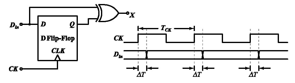
In the circuit shown below, a positive edge-triggered D Flip-Flop is used for…
GATE · 2018 · EC · Electronics and Communication Engineering
In the circuit shown below, a positive edge-triggered D Flip-Flop is used for sampling input data D_in using clock CK. The XOR gate outputs 3.3 volts for logic HIGH and 0 volts for logic LOW levels. The data bit and clock periods are equal and the value of ΔT/T_CK = 0.15, where the parameters ΔT and T_CK are shown in the figure. Assume that the Flip-Flop and the XOR gate are ideal. If the probability of input data bit (D_in) transition in each clock period is 0.3, the average value (in volts, accurate to two decimal places) of the voltage at node X is _________.
Attempted by 1 students.
Sign up free to check your answer
Sign up freeLoading lesson…