

Consider the 8085 instruction IN 09H stored as follows: Source correction: the…
PYQ GATE 2000Modified — slightly modified from the official paper; see the solution
Consider the 8085 instruction IN 09H stored as follows:
Source correction: the surviving paper reproduction prints DA at 3050H; this table uses DB because DB is the 8085 opcode for IN.
Memory Address | Machine Code |
|---|---|
3050 | DB |
3051 | 09 |
And the following incomplete timing diagram for the instruction:
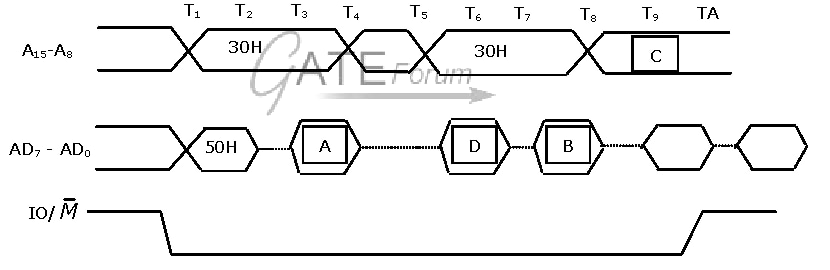
For the I/O-read cycle T8–TA, read IO/M as high; the surviving reproduction prints its IO/M trace incorrectly.
(a) Write the contents of the boxes, A, B, C and D in hexadecimal in your answer sheet. Do not draw any pictures.
(b) Write the state of both ALE and RD̅ pins at time units T1, T2, T3 and T4.
(c) How do you generate the signal that tells the peripheral to put the data on the bus? Answer by completing the following statement in your answer book:
By combining signals …………….
Sign up free to check your answer
Sign up freeLoading lesson…