Figure I shows a 4-bit ripple carry adder realized using full adders and…
GATE · 2017 · EC · Set 2 · Electronics and Communication Engineering
Figure I shows a 4-bit ripple carry adder realized using full adders and Figure II shows the circuit of a full-adder (FA). The propagation delay of the XOR, AND and OR gates in Figure II are 20 ns, 15 ns and 10 ns, respectively. Assume all the inputs to the 4-bit adder are initially reset to 0.
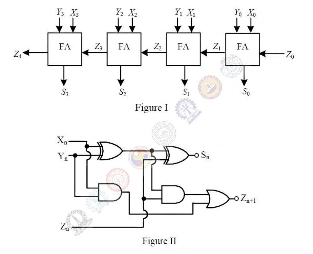
At , the inputs to the 4-bit adder are changed to , and . The output of the ripple carry adder will be stable at (in ns) = ________.
Attempted by 5 students.
Sign up free to check your answer
Sign up freeLoading lesson…