

(a) Consider an 8085 based system operating with the following specification:…
PYQ GATE 1991Modified — slightly modified from the official paper; see the solution
(a) Consider an 8085 based system operating with the following specification:
Crystal frequency : 6 MHz
ROM map : 0000 through 07FF
RAM map : 1000 through 17 FF:
ROM requires one wait state.
RAM requires no wait state.
Determine the instruction cycle time for each of the following instructions:
(i) ORI 22H
(ii) DCR M
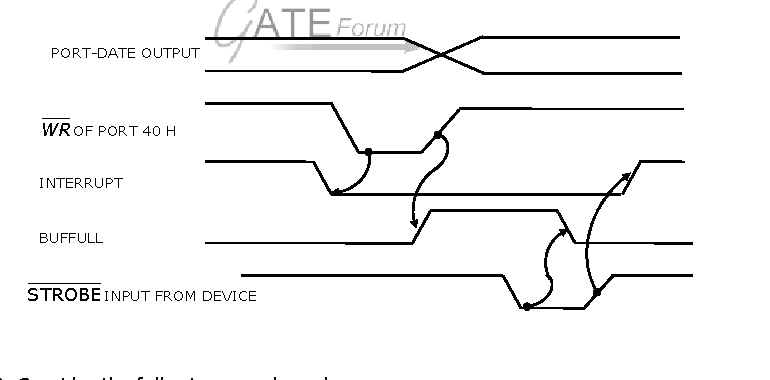
Assume all instructions and immediate bytes are fetched from ROM, the 8085 READY signal inserts one wait state into each ROM memory-read machine cycle, and all I/O control signals use the active-low polarities drawn in the timing diagram. Assume the following initial conditions of the CPU registers (in hex) for each of the instructions:
A = 55, B = AA, C = F7, D = 10, H = 10, L = FF, PC = 0200, SP = 17F0.
(b) Developing an output port interface (draw a block schematic) for an 8085 based system with a demultiplexed address bus which incorporates a handshake protocol as per the timing diagram given in figure. The interface should include a status input port at I/O address 40H which reads the INTERRUPT and BUFFFULL signals through the most significant bit and the least significant bit, respectively. The output data port is at the same I/O address 40H and is activated by a write operation. Assume the availability of SSI and MSI level components only.
Write a short program segment which performs a 200 H byte programmed I/O data transfer to the device from memory address 3400 H,
Sign up free to check your answer
Sign up freeLoading lesson…